3-Level Flying Capacitor Multilevel Inverter
Designing a wirelessly-chareable RC Car with an FCML and resonant converter.
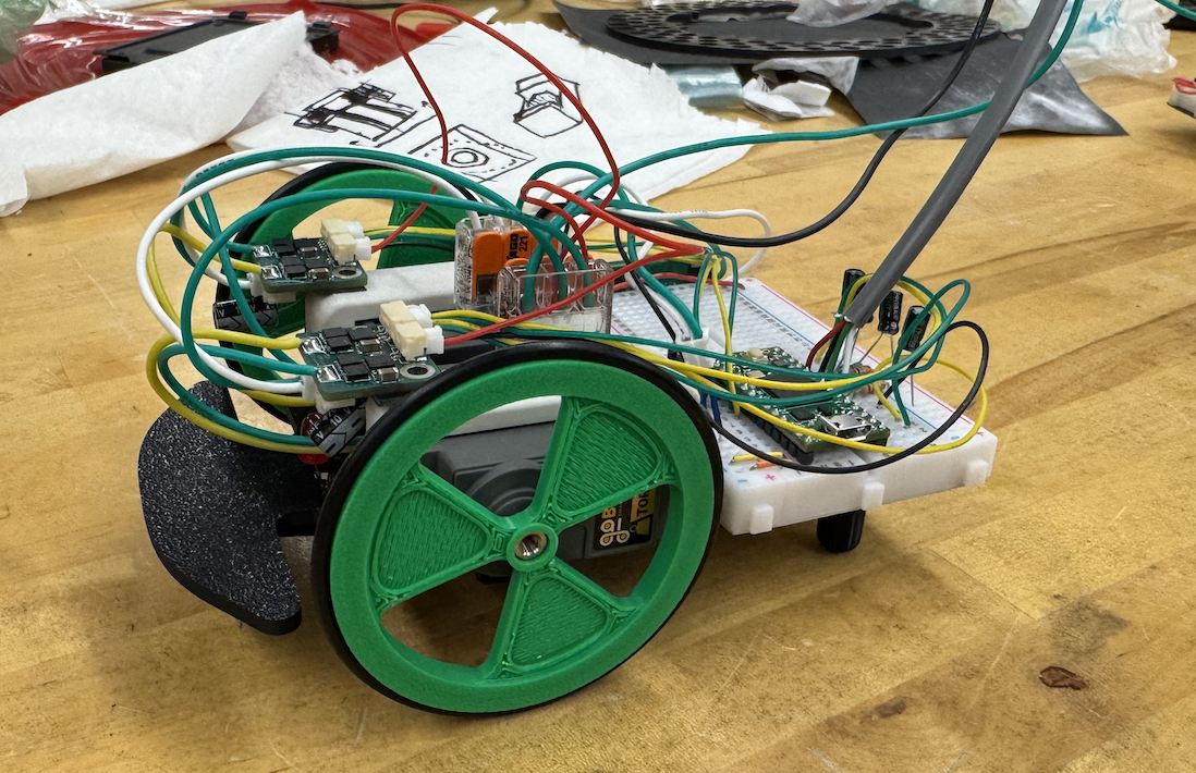
This term, I took 6.131 Power Electronics at school. The final project is open-ended, requiring you to make something interesting with a “story” that implements a couple power converters (the primary topic of the class). My “story” was kinda lame and made up - a wirelessly chargeable RC car - but it let me make some cool electronics, most notably a three-level flying capacitor multilevel inverter. Since all of the electronics (other than random wiring) is on PCBs, I was able to simplify a lot of the assembly and the entire project only took around three weekends. My final report is here, but I’m copying over all the juicy bits (design / validation of the FCML, charging setup, and flyback converters) into this post, so it’s a bit long - sorry about that. Some of the analysis / experimental validation is unfinished, so I might add to that over winter break.
Before I go any further, there were also few technical constraints:
- No batteries (apparently some people got hurt at some point), which is why everything is powered off the bench supply
- Maximum working voltage is 36V - I did everything at 12V to keep things simple and so that I’d avoid accidentally frying something.
For the report, we were also required to show all of the math / steps into designing each converter, which is why it’s a little pedantic, unlike my usual posts. Hopefully you’ll bear with it!
The charger is consists of a set of coupled inductors, one on the car and one on the ground (the “charging station”), with the transmitter driven by a 3-level FCML. The converter is controlled in open-loop by a Nucleo STM32 development board, which is responsible for setting each switch state, although the PCB has outputs for closed-loop control. In normal operation, the FCML outputs a $\approx43kHz$ three-level squarewave to drive the charging coils, which are resonant around $45kHz$.
The following discussion will cover the design of the FCML bias supplies, the FCML itself, and the charger. Experimental data is provided to verify that they work properly.
Bias Supplies
Flyback converters were a natural choice for the bias supplies since they are isolated and require few components. Using a set of three coupled inductors provides a second output without the need for additional components, so I found a 1:1:1 coupled inductor from CoilCraft. I’m using the LT3002 flyback controller for closed-loop control over the output. Instead of requiring optical feedback, this chip samples the primary-side flyback waveform for a scaled approximation of the output voltage, and regulates the duty cycle based on that. It also has an integrated switch, allowing me to reduce component count further.
Design requirements:
- 12V Input
- 10V Output
- 1A Output
In lieu of solely using the equations in the datasheet to calculate component values, I’m going to try to relate those equations to the ones from class to demonstrate their similarities. The following equations are in order of those given in the datasheet:
Step 1: Calculate the transformer turns ratio. In the datasheet, this is given by
\[N_{PS}<\frac{65-V_{IN(Max)}-V_{LK}}{V_{OUT}+V_{F}}\]This is meant to constrain $V_{SW}$ to under the maximum threshold ($V_{SW(max)} = 65V$) while preserving a margin of $V_{LK}$ for the leakage inductance spike, which is easier to see in this form:
\[N_{PS}(V_{OUT}+V_{F})+V_{IN(MAX)}+V_{LK} < 65V\]I will ignore this and use a 1:1 transformer ($N_{PS}=1$) since that should give plenty of margin.
Step 2: Calculate the minimum magnetizing inductance. Since the LT3002 samples the primary-side voltage waveform when the secondary current is zero, it actually operates in boundary conduction mode. As a result, the magnetizing inductance is chosen to limit the maximum switching frequency of the device such that it has enough time to sample the waveform. This actually just comes down to applying $V=L\frac{\Delta I}{\Delta T}$ for the $DT$ and $(1-D)T$ periods. The sampling times are $t_{off}=350ns$, $t_{on}= 160nS$. $I_{SW(MIN)}=0.87A$. Thus, to satisfy the $DT$ interval:
\[L\geq \frac{160nS*12}{0.87}=2.2*10^{-6}H\]and the $(1-D)T$ interval:
\[L\geq \frac{350nS*(12+0.8)}{0.87}=5.1*10^{-6}H\]I chose a $22\mu H$ 1:1:1 coupled inductor to stay clear of these constraints and reduce ripple current.
Step 3: Choose output diode. There are three considerations in selecting the diode. Here I list them and elaborate based on the requirements of my converter:
- It can block the secondary voltage during the primary charge state. Since I’m using a 1:1:1 transformer, the maximum expected secondary voltage is
- It can pass the necessary forward (output) current. Per the design requirements, the maximum output current is $1A$
- It has low reverse recovery time (lower than the switching period). Choosing a schottky diode makes satisfying this assignment trivial, since they generally have practically no reverse recovery time $\tau_{rr} \approx 0$. In addition, $f_{sw(max)}\approx 400KHz$ for this chip, which is relatively low
Based on these constraints, I chose the SK220A Schottky diode, which has a max forward current of 2A a maximum reverse blocking voltage of 200V, and a forward voltage drop of $0.8V$.
Step 4: Choose the output capacitor. To do this, nominal duty cycle and switching frequency must be calculated first. Since
\[V_{out}=\frac{DV_{in}}{N_{PS}(1-D)}\to D = \frac{V_{out}}{V_{in}+V_{out}} = \frac{(10+0.8)N_{PS}}{(10+0.8)N_{PS} + 12}=0.47\]To calculate the switching frequency:
\[T=T_{on}+T_{off} = \frac{L*I_{sw}}{V_{in}} + \frac{L*I_{sw}}{V_{out}+V_{F}}=22\mu H * 0.87A *\left( \frac{1}{12}+\frac{1}{10+0.8} \right) = 3.4\mu S\]Thus, $f_{sw(nom)}=297KHz$. From here, we simply have
\[\Delta V=\frac{I_{out}DT}{C}\]I chose $C = 47\mu F$ for $\Delta V = 0.03V$.
Step 5: Select the feedback resistor: This is specific to the chip, so using the equation given in the datasheet and choosing $R_{ref}=10k\Omega$:
\[R_{fb}=\frac{R_{ref}*N_{PS}*(V_{out}+V_{f})}{V_{ref}}=\frac{10k\Omega*10.8}{1}\approx 100k\Omega\]

Since the input voltage is relatively low compared to the maximum switch pin voltage, I opted to use a DZ clamp (set to $60V$; $V_{SW(max)}=65V$) in parallel with an RC snubber instead of the RCD clamp taught in class. This was done following the procedure given in the LT8302 Datasheet after I received the PCB:
- Add capacitance across the magnetizing inductance until the ringing period roughly doubles
- Compute the parasitic capacitance
- item Compute the leakage inductance
- item Calculate the snubber resistance to critically damp the parasitic LC circuit: $R = \sqrt{ \frac{L}{C} }$
The effectiveness of the clamp:

FCML Design
Motivation for FCMLs
Multilevel converters are growing in popularity for their ability to efficiently handle high voltage and frequency operation. Traditional two-level inverters place high stress on the output switches due to high $V_{DS}$, which is typically correlated with greater $R_{DS(on)}$ (higher conduction losses), and require high switching frequency $f_{sw}$ to reduce total harmonic distortion (THD) on the output1. Output switches can be connected in parallel to distribute current among individual switches and simplify cooling requirements. However, this approach introduces a timing challenge, as the turn-on of each parallel switch must be carefully synchronized2to ensure effective operation at high frequencies. Similar strategies (and issues) arise when placing switches in series to reduce $V_{DS}$.
The multilevel converter is and elegant solution to these problems. By establishing known node voltages between each switch, designers can precisely set $V_{DS}$ to lower voltages, which naturally reduces $R_{DS(on)}$ and thereby conduction losses. This reduces the stress on any given switch, thereby dismissing the need for multiple switches at each stage. Most multilevel converters also lend themselves neatly to commutation patterns which “overlap” switch states - that is, it is unlikely that any switch needs to toggle consecutively - which decreases the necessary $f_{sw}$ for the switches despite maintaining a commutatoin frequency of $f_{sw}$. This, of course, reduces switching losses. Finally, the multilevel output allows tighter approximation of most output waveforms, reducing unwanted harmonics in the output and thereby decreasing THD3. This allows weaker LC output filters, decreasing space requirements and reducing conduction losses. Typical multilevel converters in industry involve between 9-14 levels.
The flying capacitor multilevel converter establishes known node voltages between the switches with a floating capacitor charged to a known fraction of the rail voltage depending on the number of converter levels. Charging occurs naturally4 during commutation, although resistors can be used to pre-charge the capacitor(s) to their levels prior to operation, which is what my design implements. Other common topologies include the cascaded h-bridge inverter and the diode-clamped inverter.
Although the effects of higher $f_{sw}$ and multiple levels on THD should be intuitive, proving it analytically is \href{https://ieeexplore.ieee.org/document/5311996}{involved}. I opted to use numerical methods5 to show the benefit of multiple levels and switching frequency instead. Figure \ref{fig:fcvslevels} clearly demonstrates the benefits of increasing switching frequency and output levels, with both reducing total harmonic distortion, as expected.
$f_{s}=50Hz$ Demonstration of multilevel PWM model driving RL Low-Pass:

Effect of $n$ levels and $f_{sw}$ on the THD of the output

Design
Although my FCML is designed for a maximum working voltage of $18V$ - orders of magnitude lower in voltage than they are typically used for - it mimics the topology of industry designs in using isolated gate drive stages and bias supplies for each mosfet in the extended totem.

Since I chose to make a three-level inverter (the simplest type, since only one additional level at $\frac{V_{Batt}}{2}$is injected), the switch commutation order is trivial. Given the “location” of the flying capacitor(s), there are two clear constraints:
- Q2 and Q3 cannot simultaneously be on, or the capacitor will be discharged from $\frac{V_{Batt}}{2}$ without going through the load
- Q1 and Q4 cannot simultaneously be on, or the capacitor will be charged from $\frac{V_{Batt}}{2}$ without going through the load
Thus, $Q_{2}=\overline{Q_{3}}$ and $Q_{1}=\overline{Q_{4}}$. In describing the commutation order, I will refer to $Q_{2}=\overline{Q_{3}}$ as state $A$, and the negation thereof as $\overline{A}$. Similarly, I’ll use $B$ for the $1, 4$ pair.
- $A; B$: $V_{out}=V_{Batt}$
- $A; \overline{B}$: $V_{out}=\frac{V_{Batt}}{2}$; $V_{flying}\uparrow$6
- $\overline{A}; \overline{B}$: $V_{out}=0$
- $\overline{A}; B$: $V_{out}=\frac{V_{Batt}}{2}$; $V_{flying}\downarrow$7
Conveniently, the $A$ and $B$ states are cyclical and offset by 90 degrees in phase. That means both states can be PWM timer pins, thereby simplifying the code. The switching frequency can simply be set with the timer prescaler and autoreload register, which I can easily do in CubeMX since I’m using an STM32 microcontroller.
Although I only control the FCML in open loop, the fact that the $A$/$B$ states can be controlled with timer pins lends itself to a simple implementation of closed-loop control. Managing the voltage of $C_{flying}$ is done by changing the relative difference in time between states 2 and 4 (since those correspond to charging and discharging the flying capacitor), which can be done by changing the duty cycle of the PWM output.
It is important to consider that the stability of the flying capacitor voltage (and thus the entire converter) is extremely dependent on the capacitor voltage staying, nominally, at $\frac{V_{Batt}}{2}$. This equivalently assumes that the charge gained and lost during states 2 and 4 is equal. If given a DC load, this is an easy assumption to make; the load $R$ is constant for both states, allowing the capacitor to charge and discharge with $\tau = RC$. This is not the case for a reactive load (which the inductive coil is), which makes closed-loop control over $V_{flying}$ imperative and my open-loop version ill-suited for this problem8.
The isolated gate drivers I’m using are the UCC23511B, which achieve logic isolation with an e-diode. They don’t use light for their operation, which makes them faster (propagation delay is on the order of $nS$, while optical components typically switch on the order of $\mu S$), and apparently last longer. The driver is turned on with a logic-level mosfet since it requires $50mA$ forward current to turn on, a bit more than GPIO pins are typically capable of.
\begin{figure}[hbt!] \centering \includegraphics[width=0.6\textwidth]{images/isodrive.png} \caption{\label{fig:isodrive}Schematic for the isolated gate driver.} \end{figure}
FCML Testing
I began by testing the converter at very low frequency - around 150Hz - with a $1k\Omega$ load. To test the similarity of commutation states 2 and 4 (which should be roughly the same voltage, except that one state charges $C_{flying}$ while the other discharges it). I placed the commutation states successively, leading to the following output voltage waveform ($f_{sw}=150Hz$, $Z_{load}=1k\Omega$):
Which looks roughly as expected! The slight deviation in the voltage between state 2 ($A; \overline{B}$: $V_{out}=\frac{V_{Batt}}{2}$; $V_{flying}\uparrow$) and 4 ($\overline{A}; B$: $V_{out}=\frac{V_{Batt}}{2}$; $V_{flying}\downarrow$) suggests that switch 3 isn’t fully saturated, and current is flowing through the body diode instead (the forward drop is $\approx1.2V$, which agrees with the oscilloscope reading). This would be inefficient for a higher power system, but is permissible for my application. The transient during the switching between the two states is because all the switches need to be flipped, so there is a (very short) dead time when nothing is on.
Decreasing the switching frequency and load resistance allowed me to clearly demonstrate the charging / discharging of the flying capacitor. Recall that after the high voltage peak, the states are 2 ($C_{flying}$ charging), then 4 (discharge); during state 2, the load is clearly driven by the capacitor (RC dropoff), yet state 4 begins at roughly the DC rail voltage (same voltage as state 1), demonstrating that it charged during state 2. The average voltage of states 2 and 4, of course, is $\frac{V_{Batt}}{2}$, which is what the flying voltage converges to for high switching frequency.
Using the aforementioned 90-degree offset PWM scheme, I tested proper converter operation at $142kHz$, with output. Note that an output filter was omitted here for clarity of testing. The charging coil is an inductive load, so transients should mostly vanish after complete assembly.
FCML at $f_{sw}=10Hz$, $Z_{load}=1k\Omega$; charging discharging of $C_{flying}$ is clear:
FCML at $f_{sw}=142kHz$, $Z_{load}=1k\Omega$:

Charging Coil Design
To wirelessly “charge” my RC car, I used a set of 1:1 inductive coils driven at resonance to maximize their energy output and a full bridge rectifier on the receiving end to turn on an LED. Since inductors, when factoring in their parasitic capacitance, naturally have very high resonance frequencies, I placed a capacitor in parallel with each one to create an LC “tank” with lower resonant frequency. \newline
Principle of Operation
Consider driving the coil directly. If the output impedance of the source voltage is $R$, it forms an RL high-pass filter with the coil with cutoff frequency \(\omega_{c}= \frac{R}{L}\) Assuming that the inductor is driven by a sinewave, the voltage across the inductor is proportional to the amplitude of the current flowing through it, so a clear constraint in maximizing the inductor current is requiring $\omega>\omega_{c}$. Since $L$ is on the order of $\mu H$, however, $\omega_{c}$ tends to be high\footnote{During testing, $\omega_{c} \approx 1MHz$}. This is undesirable since a higher switching frequency increases stress on the FCML. Decreasing $\omega_{c}$ requires either a high inductance (impractical to design and results in higher conduction losses) or a lower source impedance (that is, a higher output current). In the context of this project, increasing the output current is particularly undesirable since it is limited by the size of the flying capacitors, which I’d prefer to keep small.
Adding a parallel capacitor to the inductor makes the system a band-pass filter, with the passband occurring at resonance and maximizing the gain at 0 decibels: \(V_{out}=V_{in} \frac{sL}{s^2RLC+sL+R}\) The oscillatory current in the LC network is simply given by
\[\frac{d}{dt}(Q=CV)\to i=C\frac{dV}{dt}\]and is proportional to the amplitude of the input sinewave $V_{0}$ (much easier to control, in my case).
This analysis isn’t comprehensive given that the FCML has a reactive output during states 2 and 4, however. Since those states involve the discharging of the flying capacitor, the impedance of the transmission circuit changes. Modeling the system as a capacitor in series with the resonant tank:
\[Z = \frac{1}{sC_{flying}}+\frac{sL}{s^2LC+1}=\frac{2s^2L(C+C_{flying}) + 1}{sC_{flying}(s^2LC+1)}\]Presents conjugate imaginary zeros at
\[s=\pm \frac{j}{\sqrt{ 2L(C+C_{flying}) }}=\pm j\omega_{z}; \omega_{z}=\frac{1}{\sqrt{ 2L(C+C_{flying}) }}\]This is problematic, since (as mentioned previously), the output current is limited by the capacity of the flying capacitor. It is thus favorable for $w_{r}\gg \omega_{z}$, which is the case when $C_{flying}\gg C$.
A series resistor is effective in damping this negative peak (it actually makes the zeros conjugate complex, which means that no sinusoid can excite them! Isn’t that sick?). In lieu of solving for the new zeros, I present the bode plot for each solution for comparison in Figure \ref{fig:bodes} with my chosen values of $L, C, \text{and } C_{flying}$. The bode plot shows the negative peak to occur around $2kHz « 45kHz$, which is sufficiently low to avoid using a series resistor. That said, the inductor gets very hot during normal operation, so it likely makes sense to use a series resistor for the purposes of reducing the power dissipation.
Bode Plots of the above transfer functions. Note that all have the same LC resonant peak:

Construction
I wound my own circular (2 inch diameter) air-core planar inductors using 45 loops of 26AWG wire, achieving a measured inductance of roughly $127\mu H$ in both. I used a $100nF$ capacitor, in parallel with the inductors, to achieve a resonant frequency of $\approx 45kHz$. The receiver side simply has an LED soldered in parallel. For practical applications, it likely makes sense to use a full bridge rectifier after the inductor output for improved efficiency, however this proved unnecessary to satisfy the requirements for this project, so I was a litle lazy. Since $C_{flying}=44\mu H \gg C = 100nF$, using a resistor was unnecessary.
Video
-
Practical implementations involve lower $f_{sw}$ with more aggressive output filters to reduce losses. Unfortunately, this simply converts switching losses into conduction losses with marginal benefit ↩
-
In practice, this is difficult to do due to parasitics, specifically, trace inductance on PCBs. ↩
-
This serves two benefits: 1) Lower necessary switch frequency, since higher switch frequency allows a better approximation of a sinewave, and (assuming the inverter is used to drive a motor) 2) Lower core losses. Marginal benefits are also achieved with lower current ripple, which may result in slight conduction loss due to the skin effect. ↩
-
Closed-loop control over the flying capacitor voltage is still a (somewhat) open problem in research. The output current capability is limited by the flying capacitances, making the design of professional FCMLs a balance between space and power output. Multiple control and sizing strategies have been devised to optimize this. ↩
-
Pulse-width modulation waveforms were generated given an input (target) sinewave and a switching frequency, and the DFT was taken to examine their frequency content. An output filter on the converter model was omitted to make the data more clear at the expense of practical THD modeling. ↩
-
The switch states create an RC charging circuit, causing $V_{flying}$ to increase. ↩
-
The switch states create an RC discharging circuit (no source voltage) causing $V_{flying}$ to decrease. ↩
-
That said, it should be noted that reactive loads can be approximated as purely resistive for $f_{sw} \gg f_{0}$. ↩