After nearly three weeks of waiting (digikey parts came in super late due to a lab financial mixup) everything finally came in.
Forword: I need to thank my lab mentor, Chris Shallal, for helping me out on this project, especially on the human-bio side of things. He’s the reason I didn’t accidentally electrocute myself :D
I spent about a day soldering everything with a new metcal soldering iron I bought on eBay and tested it out on the weekend, starting with the flyback converter. I was concerned that this wouldn’t work since I designed it pretty hastily and bought a few insanely cheap ±200V flyback converters on amazon. Seeing something that cheap and “sus” charge to 350V is pretty crazy:

Have I mentioned that flyback converters are really cool? They’re inherently isolated (one of the reasons I chose them for this, since IEC 60601 mandates this) so providing feedback to the controller can be tricky. Most chips use optocouplers, but the LT8304-1 samples the primary-side coil back-EMF. Pretty cool.
Debugging
Flyback
For reference, here’s the schematic for my flyback (almost a direct copy of one of the application examples):

Initial tests of my flyback converter were a bit shaky. I don’t have any pictures of this, but basically the output voltage was much lower than expected - around 20V. Probing the SW pin showed periodic (at a frequency of 1-2Khz or so) ringings of ~2V that would dissipate, rather than roughly rail-to-rail switching, as I expected. The ringing frequency was roughly 40MHz, which was almost certainly my RC snubber (across the primary winding). The DZ snubber was getting hot though, and since it hopefully shouldn’t be necessary (1:5 transformer stepping up to 200V, so the SW pin should technically be at about 40V at steady state, giving transients a ~50Vpp margin, and this transformer has low leakage inductance anyway) I took it off. That did the trick. Looking through the documentation again, it became pretty clear that I had just specced this thing wrong. With a 15V input and a 24Vz zener, I was basically clamping at the exact steady-state voltage and (I imagine) not giving the SW pin room to deal with the initial step response in trying to start the regulator. Instead, nearly all that energy was being dissipated in the DZ snubber, leaving almost no energy for the flyback to do any voltage conversion. Hence the 20V, rather than 200V, output.

With ~2.5W input power, maximum output current should be around 10mA (easy math accounting for losses), which corresponds to a SW frequency of roughly 50Khz, based on one of the graphs. The SW pin was at 62KHz, so seems about right.
Overcurrent Latch
Next up was testing the comparator circuit. It’s not very elegant but makes use of some chips I had lying around:

Knowing the sense resistor (the one that sets the driver output current, check my previous post), a current limit can easily be set by changing R2 and R3. It’s latching because of U2 (this could actually be a mosfet, but whatevs), and the OC_SENSE is will be an output to the enable pin of the flyback converter to turn the HV off. Although I don’t have pictures of it, this worked without any stress.
Driver
This is what really matters. I first decided to try testing it out at around 3mA and 10V, since that should be low enough to get some current flowing through a 2k test load. Nothing happened. Initially, I thought this was a problem with the way I was communicating with the analog switch, which is through a simple 8-bit shift register. After about two hours of debugging (the first half of which I spent discovering that the ground strap on my oscilloscope probe broke and the second half of which I spent using the logic analyzer to make “quick work” of this problem) I concluded that my code had to be correct. As it turned out, this was a pretty simple hardware problem that stemmed from rushing through this design a bit too quickly:

I had somehow completely ignored the ±10V margin that the analog signal was supposed to have, aside from 10V being too low to do anything. Although I noticed this when looking for similar analog switches but just forgotten about it when looking at this chip! Since I ultimately aimed to switch 0-200V and hand’t paid attention to this, I’d just connected $ V_{PP} $ and $ V_{NN} $ to the HV (200V) rail. Testing at higher voltages - around 40V - yielded so much distortion in the current measurements that it was basically hopeless. So much for testing biphasic current stimulation.
I spent the next few hours looking for replacement switches, yielding nothing since practically all of those made for high voltage are meant for ultrasound, which doesn’t require rail-to-rail operation. The “easiest” solution to this problem would be to supply $ V_{PP} $ and $ V_{NN} $ with the voltages they needed, but this would require two more converters: an isolated ~-10V source, and a ~215V source (which would require another flyback). That sounds disgusting, so instead I ditched the analog switch idea altogether. This new topology is inspired by an H-bridge:

And honestly, this is way cleaner than the analog switch idea. The switches also had the additional risk of being too slow (the max shift register clock was 20Mhz for roughly 400nS commanded switching time, but even then, it feels sketchy to require a communication protocol at all). There are two mosfets on each quadrant of the H-Bridge so that I can swap test out different ones. They have different footprints.
Testing
Although the analog switch wasn’t going to work, I could still test the constant current driver. After hooking everything up on a breadboard,

It worked! The current through the 2kΩ load nearly matched what I commanded, and, as expected, the Mosfet $V_{ds}$ exactly followed this drop. I tested it up to 30mA, the design requirement, and it seemed to work flawlessly, with basically a perfect $R^{2}$ value:

That said, during this testing, I quickly noticed a problem. Although I knew the mosfet was going to get hot (max dissipation is $ 0.03 * 117.46 = 3.5W $), I smartly neglected to calculate the actual temperature increase. With a thermal junction-ambient resistance of 125°K / W, this mosfet was cooking, and I suspect that it was getting close to thermal runaway.
I slapped a small heat sink on it, and along with a 12V PC fan, things seemed to reach steady-state, for a current of 0.015mA, at around 40°C. Naturally, the second version of the driver features much larger mosfets (From TO-252 to D-Paks, these are chonkers) for a much lower $ R_{thJC} $ and more surface area for a heat sink. I’m still going to need the heat sink though.
Here’s the 40°C steady-state, measured using an overpriced FLIR camera the lab had lying around:

Transients
The next step was to make sure that the risetime of the system was good enough to actually match the timing requirements of the system. I’m ignoring the rise time of the flyback charge because that doesn’t change during stimulation, so as I mentioned in the previous post, this was just about tuning the feedback resistor / capacitors in the driver circuit:

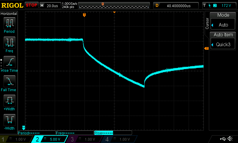
Here’s what the response looked like (voltage over the load):

At 200uS/Div, this sucks! It takes nearly 400uS (double the negative stimulation period) to reach steady-state. I really should’ve turned on cursors to measure this, but judging from the graph, it looks like the rise time should be somewhere around… 60uS? The RC loop exists between R18, C16, R20, and $ C_{GS} $ of the mosfet. $ C_{GS} = C_{iss} - C_{rss} $, so $ \tau \approx 500.2k\Omega * 170pF = 84.6\mu S $. Seems about right.
Working with the components I had, I dropped R18 to 30kΩ and C16 to 10pF. That got me a nice square:

With a stock RC-looking curve and short rise time:

Finally, just to prove that C16 was necessary to attenuate the transient, I removed it. This means that the transient response is much more dependent on the op-amp characteristics, since we’re basically just testing the negative feedback speed (which is dependent on slew rate, maximum output current, etc.) The OPA810 is pretty expensive, so let’s see how it performs:

Whadaya know! I’d rather not have 40Vpp transients… the cap is going back on.
After a night and day grinding, I sent out new boards (the ones with the H-Bridge configuration) with the confidence that the driver, at least, would work. Here’s what the cad looks like:

Stimulation
The day after everything got sent out, I realized that I hand’t even stimulated myself yet. Although I wouldn’t be able to have charge balance, DC stimulation can be used for short periods safely. I hooked up some electrodes to my