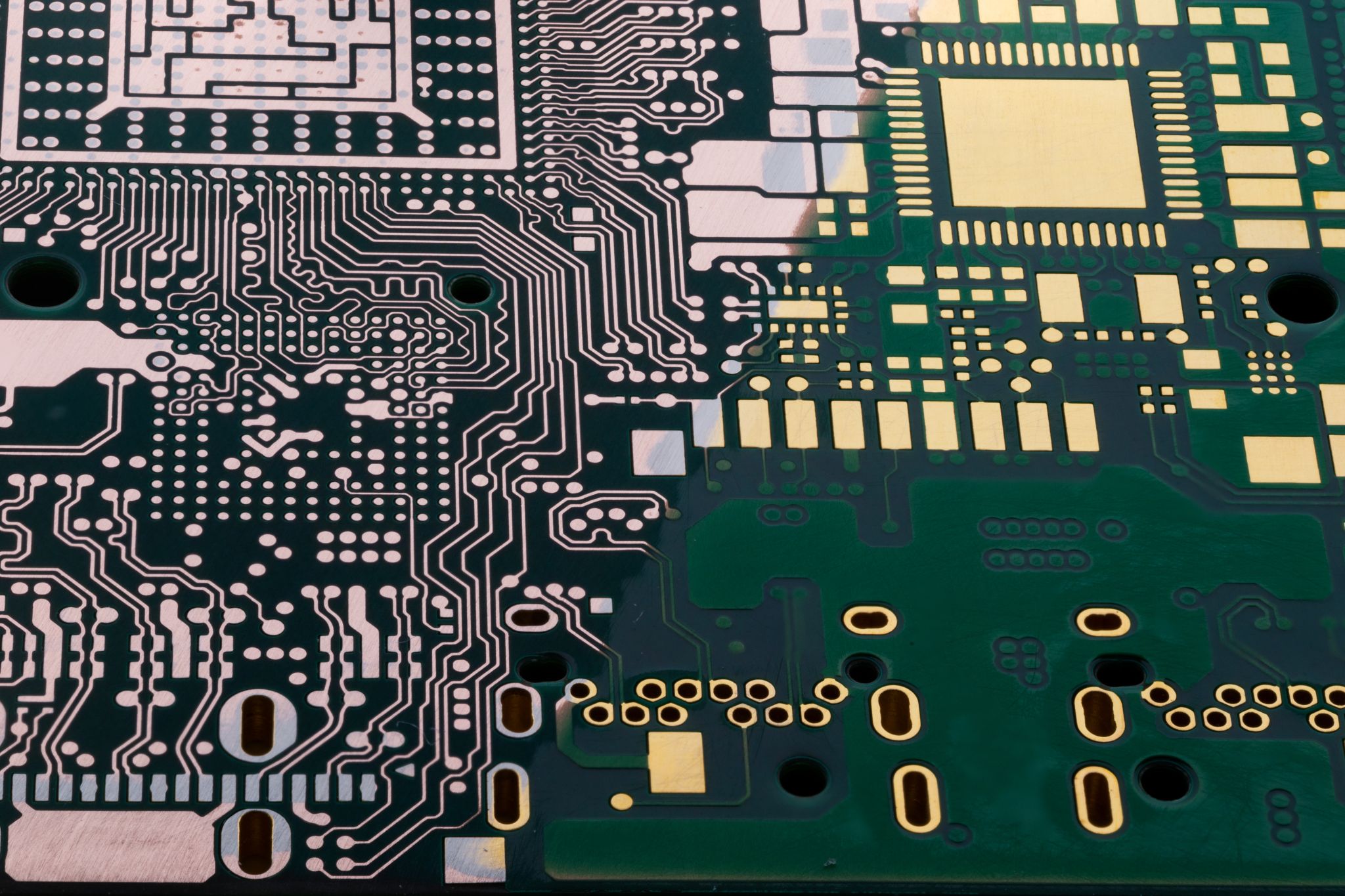
Credit to Lukas for the beautiful cover image, which I took from his linkedin post
I follow a cool EE on linkedin who tends to have pretty high-quality posts (really nice pictures, discusses something interesting, etc. can’t say that for most of linkedin…). A few weeks ago he posted this:

Most high speed boards are designed with soldermask voided over transmission lines, the general consensus being that soldermask is lossy and the process isn’t as well controlled compared to plating1. What Lukas pointed out is that ENIG introduces a highly lossy (up to 8x more lossy than copper) nickel layer that results in high skin effect loss. Covering the copper traces in soldermask means you don’t need to plate, so the loss depends mostly on the copper resistivity (which is much lower than nickel) instead. You’re balancing the nickel against soldermask, and the claim is that the thin nickel layer is worse. This effect is most clear for coplanar wave guide (CPW) since the majority of the field comes out the edges and top of the trace (where nickel is plated). You wouldn’t expect much of a difference for microstrip.
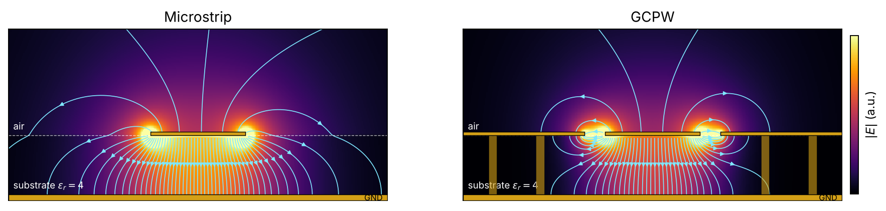
At the time I was just finishing up a coupon for a directional coupler, and I decided to throw in a test fixture to measure this myself. Traces are grounded coplanar waveguide (GCPW).
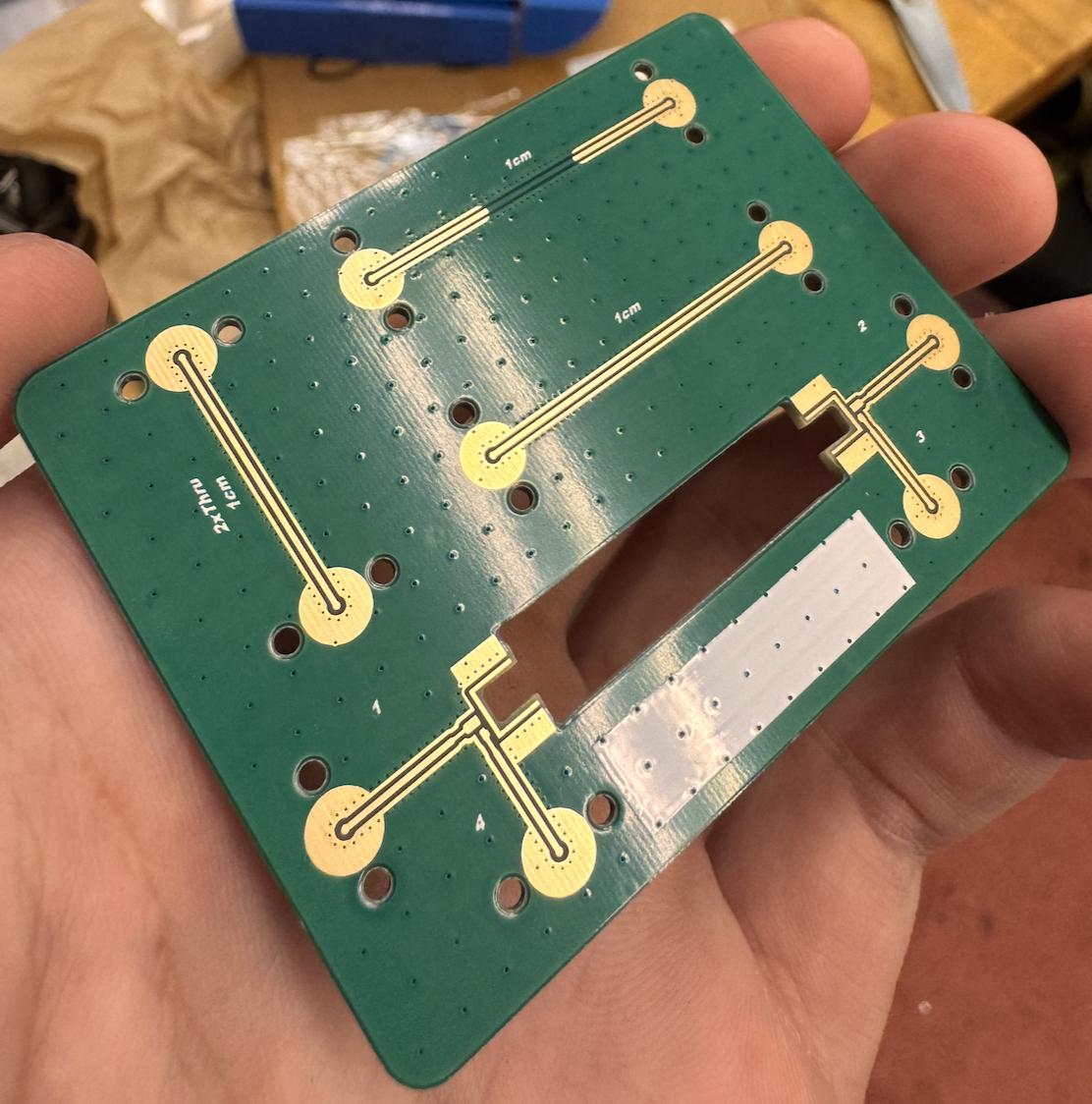
This is on jlc3313a FR4 4 layer stackup, which is by no means ‘high speed’; jlc states a df of 0.01 and dk of 4.1. Should still be good enough for test though. Though 2xThru fix-fix is at 90 degrees to the coupons (so the prepreg weave they see is different) I haven’t heard of that being a problem past 20GHz or so. Shouldn’t matter for this because largest change skin effect loss will occur at low frequency anyway.
Experiment
Measurement process here was to do a 2xthru deembedding on the longer lines, extracting 1cm soldermasked and un-soldmasked lines. Then scikit-rf has methods for computing the loss tangent via the extracted ABCD matrix.
As an aside, here’s the launch for the fixfix - it looks a lot better than before, once I added that gnd opening under the feed. Still not great, but probably good enough.
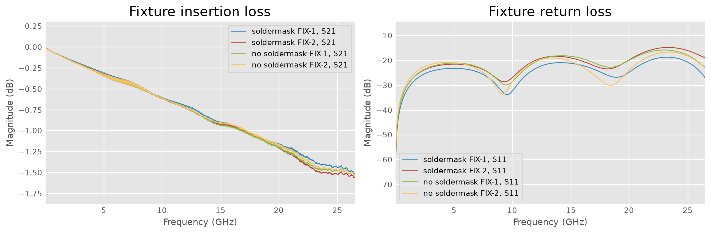
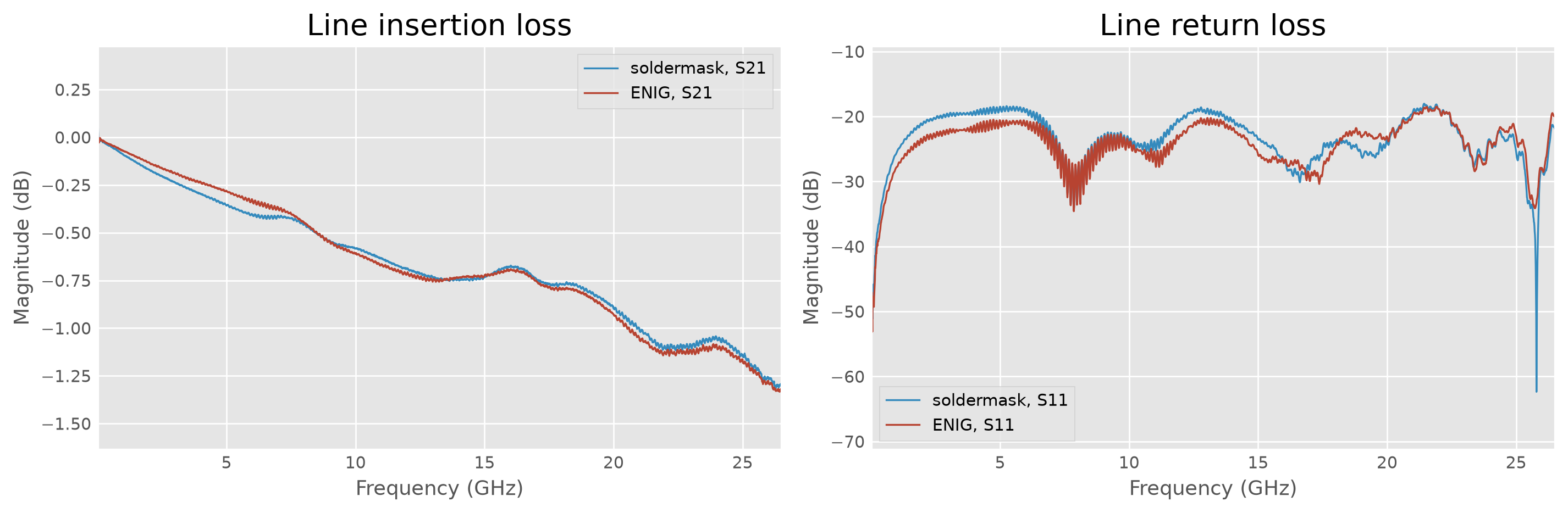
Extracted lines:
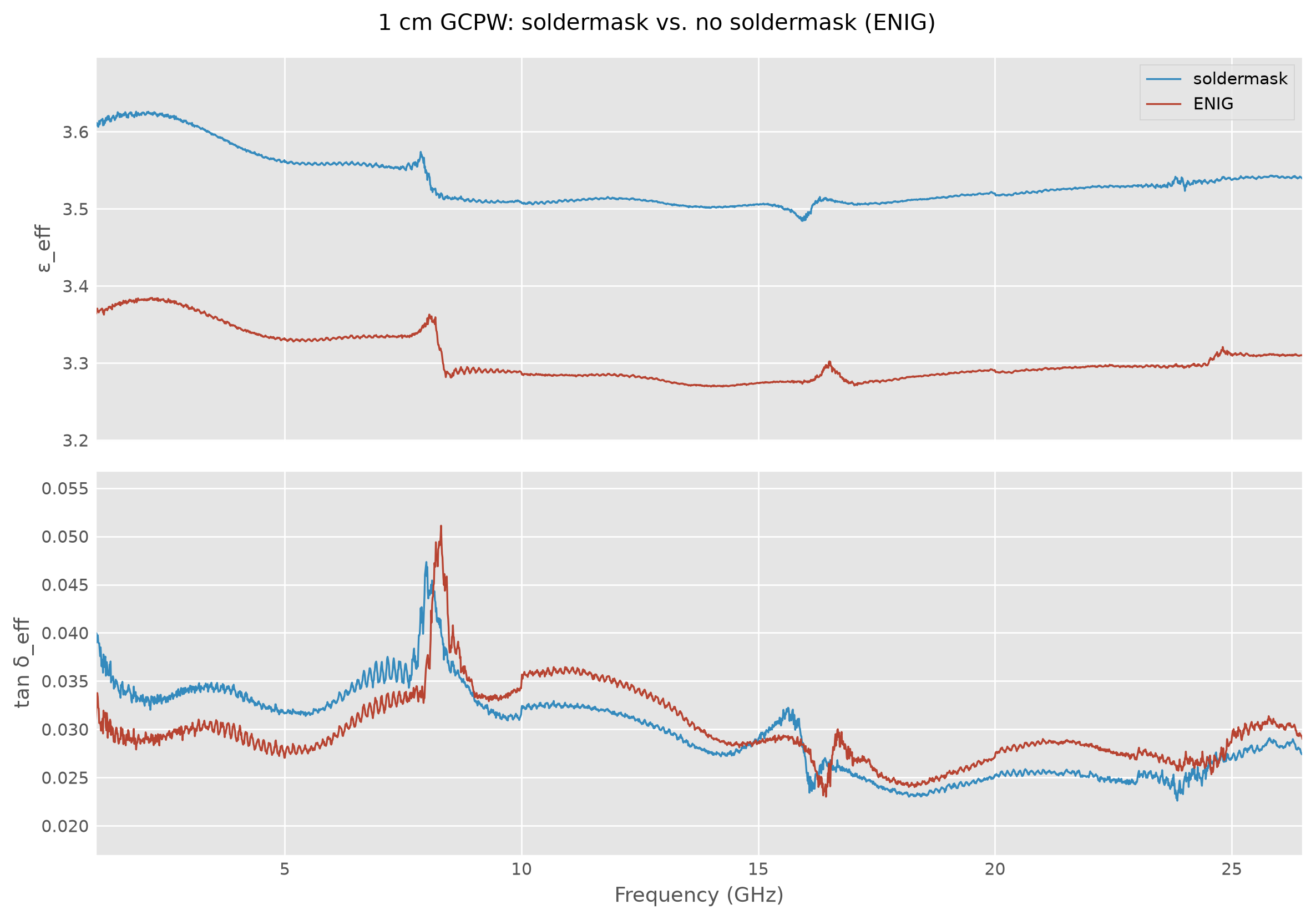
Here’s the interesting part - plotting the df / dk. As expected, the soldermask increases the effective permittivity a lot (this is the main reason to expose soldermask and plate - the trace Z0 becomes veyr dependent on the soldermask thickness, which isn’t well controlled)
You can also clearly see that the loss tangent is higher on the ENIG sample. The spiky behavior at ~8Ghz / 16Ghz corresponds to when the sample is quarter wave, resulting in the calculation becoming very sensitive to the measurement quality (so calculation is unreliable). To do some data cleanup, I fit a model to the loss term:
\[\alpha = \alpha_{c}\sqrt{ f }+\alpha_{d}f\]Where $ \alpha_{c} $ is conduction loss coefficient (skin effect is porportional to $ \sqrt{f} $) and a dielectric loss coefficient $ \alpha_{d} $. Loss tangent is then the ratio2
\[\begin{aligned} \tan\delta=\frac{\alpha}{\beta f}\sim \frac{c_{1}\alpha_{c}}{\sqrt{ f }}+c_{2}\alpha_{d} \end{aligned}\]The form demonstrates that dieelectric loss contributes a constant offset, while the skin effect loss contributes the curvature of the loss. This means that when we look at the fits,
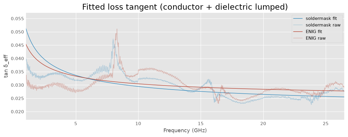
the fact that there is a clear intersection in the loss tangents at ~6Ghz indicates that skin effect is probably the dominant factor in explaining that phenomena. You would expect the intersection point to happen where the skin depth of nickel approaches the nickel plating thickness, since that’s when the current density is mostly concentrated in the nickel. To show this, I’ll plot skin depth vs nickel thickness.
It turns out nickel used in ENIG is typically 8-12% phosphorus by weight corresponding to between 70e-6Ω·cm - 110e-6Ω·cm.
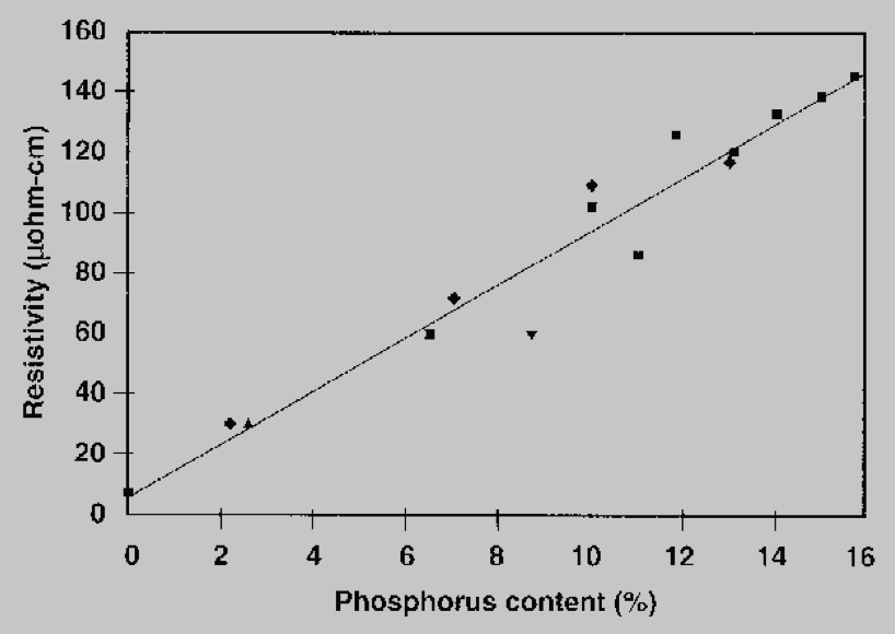 Source: Nickel Institute
JLCPCB states that their nickel layer is between 3-6µm thick. Plotting these against each other on a graph, and with the intersection:
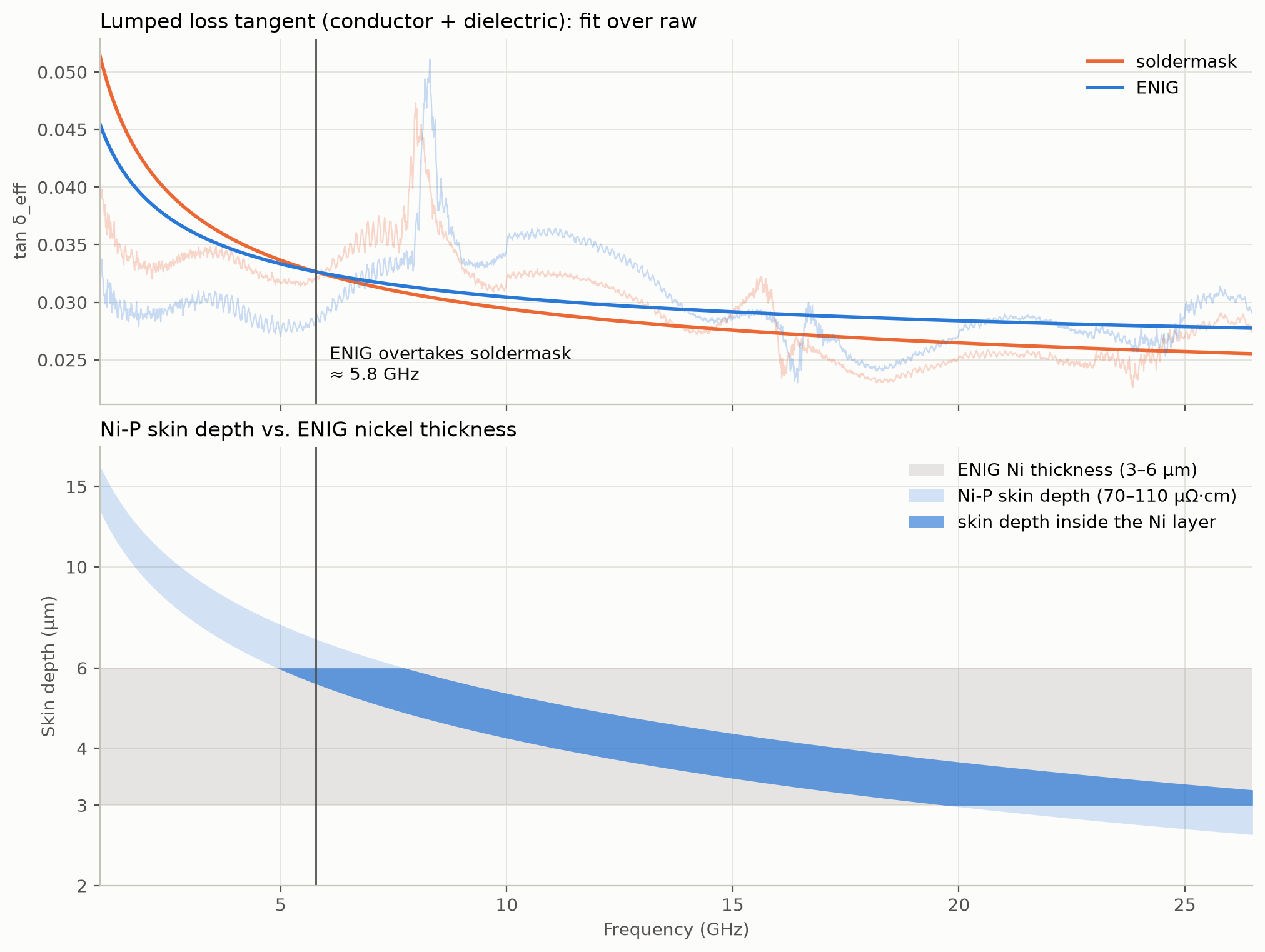
So the difference in loss can be explained by skin effect, which is pretty cool! Of course, this isn’t a super accurate experiment (I don’t know what the actual nickel thickness is, the actual resistivity, and the intersection need not necessarily occur when skin depth equals nickel thickness) but the results are pretty satisfying and do suggest that Lukas could be right.
Conclusion
Despite this, it’s probably still a good idea to void soldermask for well-controlled dk, and use different plating. OSP and immersion silver are pretty common for rf designs, though they are expensive. If you’re on a budget (like me), the ENIG is still worth it since difference in loss is so low.
If you’d like a copy of the data, let me know.
-
Poorly controlled soldermask thickness can give you varying dk, of course, which is also a big reason to void. ↩
-
Using transmission line notation for propagation constant here, with $E \propto e^{\gamma x}$ where $\gamma=\alpha+j\beta$. I always find this notation confusing from physics background because I’m used to working in $ k = \gamma / j$ ↩