It is fairly common to need to adapt between line widths on an rf board. For example, most RFIC chips have pads that aren’t the correct line length to match impedances - standardizing this would require standardizing the pcb stackup! The fix for this is to create an adiabatic taper between the two widths to prevent unwanted reflections at the mismatch. Three common taper types are the exponential, triangular, and klopfenstein types.
These tapers are simple geometry to generate but annoying to draw. Also, they are typcially defined as a function of impedance (the impedance tapers by the profile) which is somewhat unhelpful since geometry is strongly nonlinear in the impedance. This means that you can’t take the taper formulas and use them as the geometric taper on the pcb - they’re a little different than that.
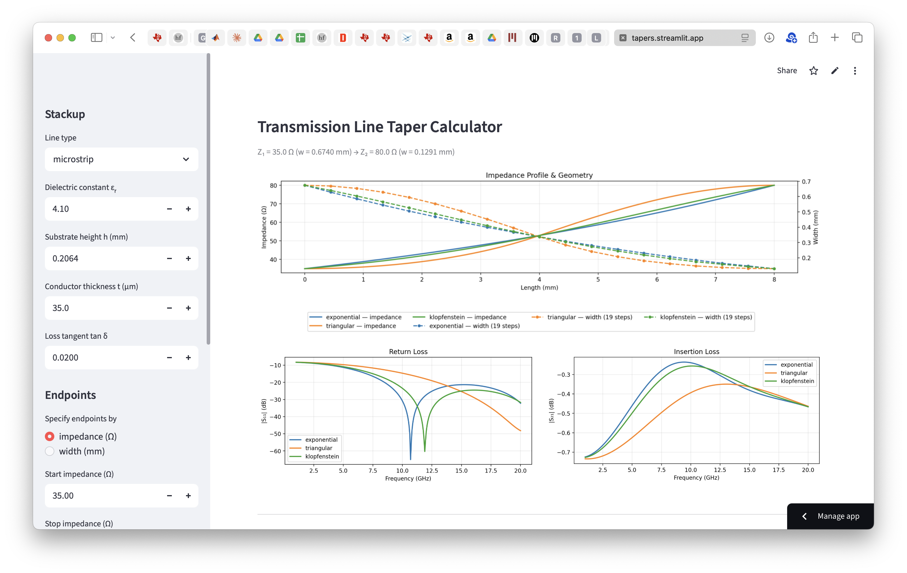
Try out the calculator!!!
tapers.streamlit.app
It supports tapers between defined impedances or widths, and the taper itself is computed in impedance using design equations from Pozar for the microstrip model and Waddel’s for the CPW with ground model. These models have practically negligible error for this application because the tapers is already extremely low loss; your analysis should be more holistic in comparing taper types and lengths. It also supports dxf and s2p export, which is super handy since all the tapers are curved.
Theory
What defines a ‘good’ taper is high return loss and low insertion loss. Reflection coefficient $ \Gamma $ on a continuous line is defined as a ratio of impedances:
\[\Delta \Gamma= \frac{(Z+\Delta Z)-Z}{(Z+\Delta Z)+Z}= \frac{\Delta Z}{2Z}\]As $\Delta Z$ tends to zero, this becomes a derivative:
\[d\Gamma=\frac{1}{2}\frac{d}{dz}\ln\left( \frac{Z}{Z_{0}} \right)\]Thus by integrating:
\[\Gamma(\theta)=\frac{1}{2}\int _{z=0}^l e^{-2jl\beta z}\frac{d}{dz}\ln\left( \frac{Z}{Z_{0}} \right)\, dz\]This is known as the theory of small reflections, and it is covered in most textbooks. The problem with this method is that it cannot handle multiple reflections or large reflections, making it fairly inaccurate for larger discontinuities.
Instead, the calculator models each small section of the taper with the ABCD matrix for a line:
\[\begin{pmatrix} A & B \\ C & D \end{pmatrix}=\begin{pmatrix} \cos(\beta l) & jZ_{0} \sin(\beta l) \\ \frac{j}{Z_{0}}\sin(\beta l) & \cos(\beta l) \end{pmatrix}\]Then you can chain all the sections together and write the reflection coefficient (or any of the s parameters) exactly:
\[\Gamma=\frac{AZ_{l}+B-CZ_{0}Z_{L}-DZ_{0}}{AZ_{l}+B+CZ_{0}Z_{L}+DZ_{0}}\]There are three types of common tapers: triangular, exponential, and Klopfenstein. In general, triangular is worst, exponential has early rolloff but passband response isn’t super good, klopfenstein is opposite with worse rolloff but best optimal passband response 1.
Hopefully this helps! I primarily made this for the dxf export functionality, and I have already used it several times for tapers out of component pads. In the future I might add openems support for more accurate impedance caluclations and s parameter extractions.
Ziad Hatab has a good explanation on this topic as well.
-
Klopfenstiein taper is a stepped chebyshev transformer with infinite steps, so chebyshev-like behavior (this slow rolloff but great passband response) is expected. ↩