While debugging the wilkinson return loss, one of the explanations I came up with for the poor response was that the impedance of the quarter wave lines was wrong. Specifically, if the λ/4 trace were wider (decreasing the line impedance for GCPW) than expected, the simulated S11 would flatten and isolation would increase, which was roughly the response I was getting. Just 25μm (from a width of 0.175mm to 0.2mm) is enough to see a difference:
| λ/4=0.175mm |
|---|
 |
| λ/4=0.2mm |
|---|
 |
I made these boards with jlcpcb, which has a 20% tolerance on trace width. 20% of 0.175 is 35μm, quite a bit.
This post is about checking those widths, and then having fun on expensive machines looking at characteristics of pcbs.
Trace widths
First, let me mention that the reason I have access to these nice tools is because I’m still in college. The two microscopes are for ‘public’ undergrad use in the breakerspace.
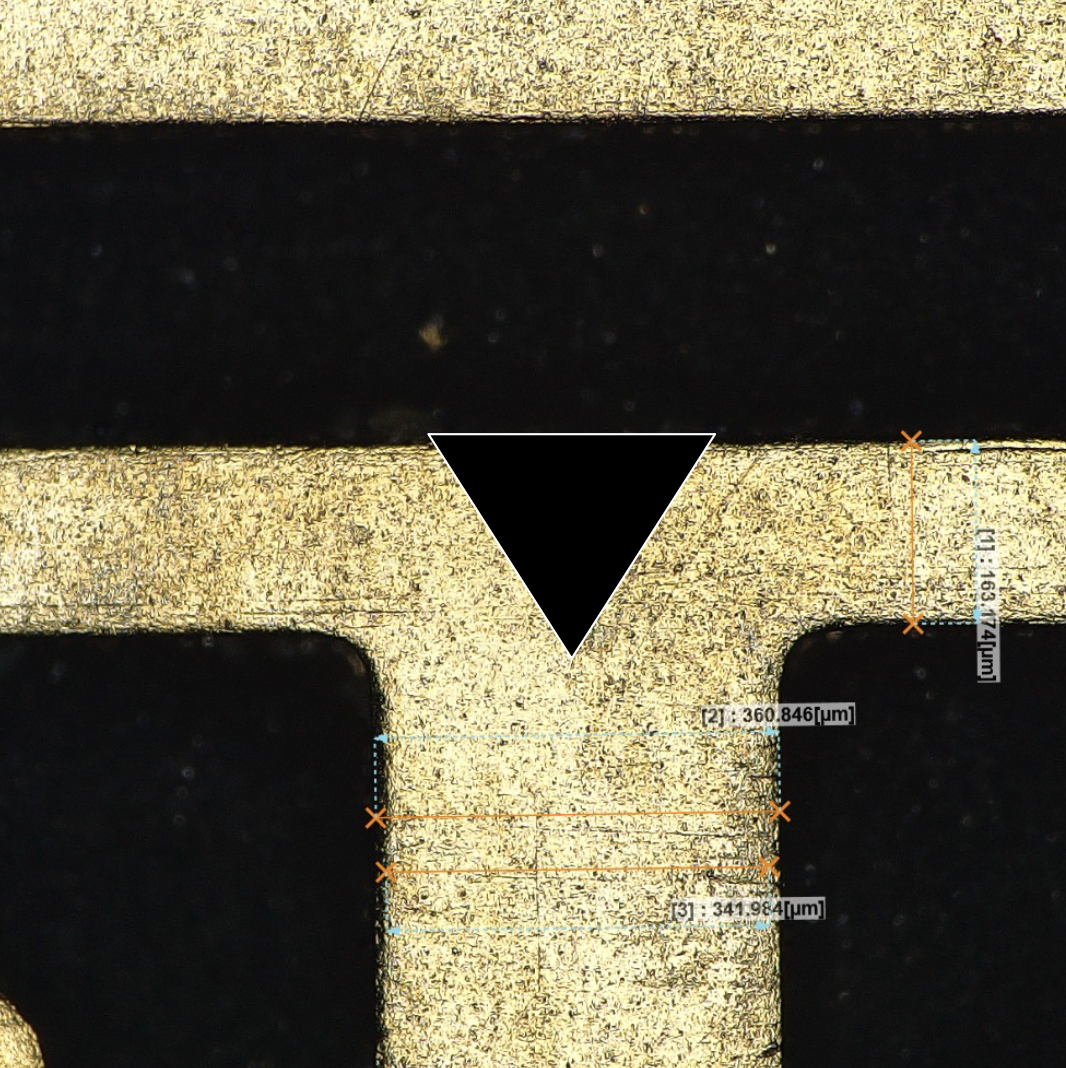
Target λ/4 width is 175μm while target feedline width is 370μm.
Optical microscope
First I stuck it under the digital microscope. One of the neat things about this machine is that you can measure distances on it. Measuring at the T junction shows the only two important trace widths on the pcb (the 50Z feedline and the 70.71Z λ/4 arm).
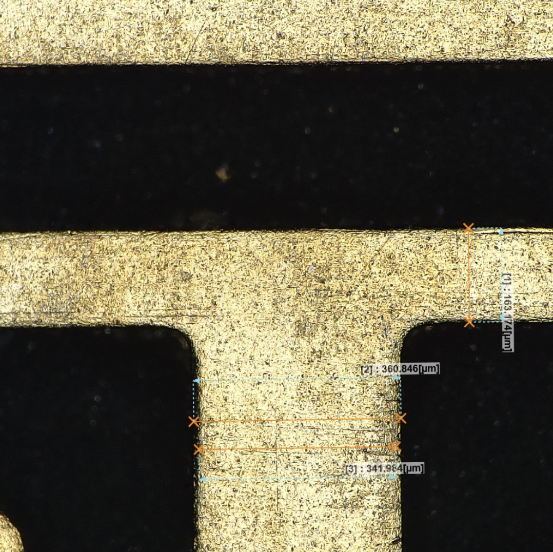
Both are easily within the jlc spec, though a little off from where I’d like. For the wider 50z arm line I took two measurements (min/max) since it’s a little difficult to see where the trace edge really starts. The edge is slightly rounded.
As an aside, with the up-close picture you can clearly see that an obvious improvement to the wilkinson would be to make the junction be composed of mitered corners going left / right to avoid the large capacitance where the horizontal and vertical meet each other. Cutout like this would probably help:
SEM
Unfortunately, the SEM doesn’t let you take measurements in the software. Instead, it gives you a scale and you’re supposed to use a pixel counter or something to align everything. I ended up just using google slides to scale the rest of the image.
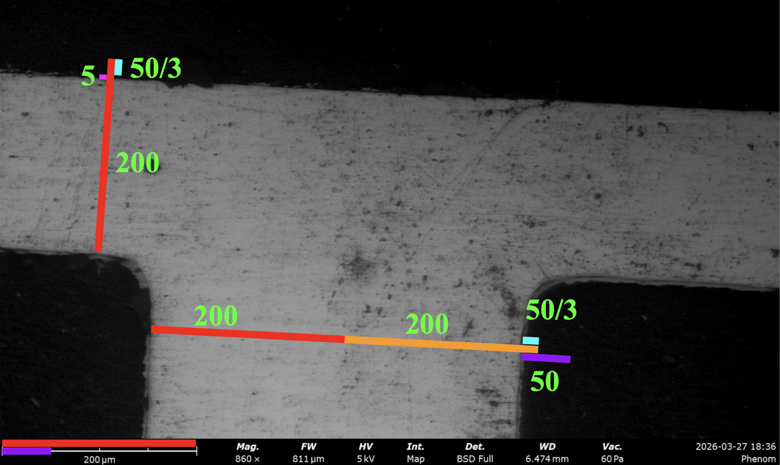
Numbers are the distances of the lines in microns and reference the scale in the bottom left. This gives a λ/4 width of 178μm and a 50z feedline width of 383μm.
What’s interesting is that the SEM measurements are consistently larger than the optical measurements, though within reason. There are a few reasons I think this might be the case:
- Sem image is taken while the board is rotated and the view isn’t exactly top-down1. Might lead to some distortion in the image on the trace edges leading to me overapproximating the width
- The optical just has a harder time seeing the edges because the illumination is from the top and the edge of the trace is slightly curved (will see later). Oblique illumination might’ve made the edges sharper.
In conclusion, though - both measurements are very close (within 10μm) of their targets, so this doesn’t explain the discrepancy in wilkinson performance.
SEM-EDS
EDS (Energy dispersive spectroscopy) is a feature of most SEMs. Here’s my rough understanding of how this works: the machine blasts the sample with electrons to eject the inner shell electrons away, and when outer shell electrons bounce into lower suborbitals to fill the energy gap, they release the difference in energy as xrays ($E=hf$, very cool). The frequency is characteristic to the orbital energy difference which is characteristic of the atom, allowing you to determine the element that just got blasted. This lets you figure out the chemical composition of the thing you blasted.
I fabbed both enig and hasl versions of my boards:
| ENIG composition |
|---|
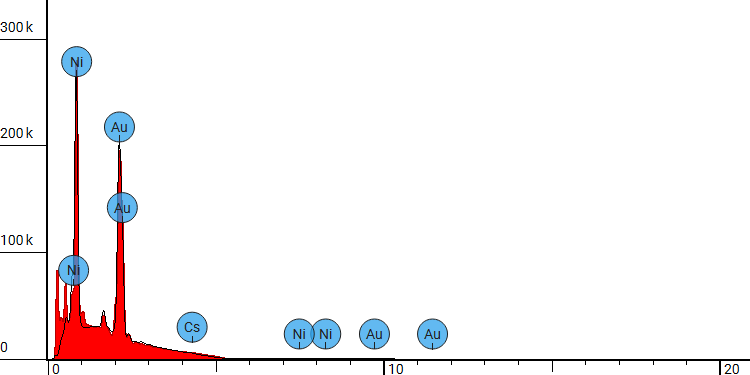 |
x axis is energy (tells you composition), y axis is x-ray counts / intensity (tells you how much).
| Atomic Number | Symbol | Element | Atomic Concentration (%) | Weight Concentration (%) | Energy Level (keV) |
|---|---|---|---|---|---|
| 28 | Ni | Nickel | 0.562869 | 0.28 | 5300 |
| 55 | Cs | Cesium | 0.0195289 | 0.022 | 5300 |
| 79 | Au | Gold | 0.417602 | 0.698 | 5300 |
ENIG stands for Electroless Nickel Immersion Gold, so the presence of nickel and gold is unsurprising. After doing some poking around online, it looks like there is no way cesium should be in there and it’s probably an identification artifact.
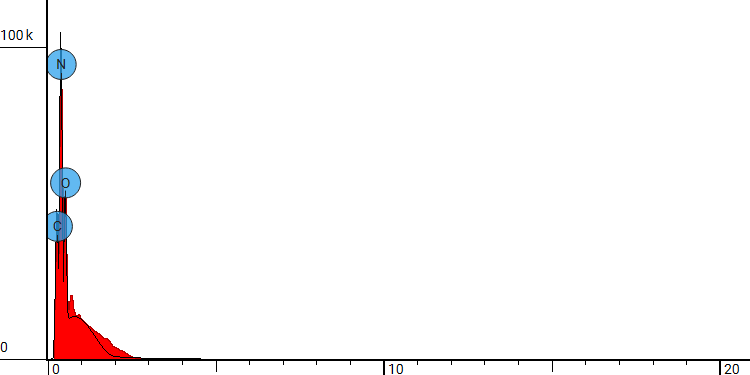
The first time I measured the HASL the measurement reported the presence of a bunch of carbon, which was just because I forgot to clean the sample:
| Dirty HASL composition |
|---|
 |
| Atomic Number | Symbol | Element | Atomic Concentration (%) | Weight Concentration (%) | Energy Level keV |
|---|---|---|---|---|---|
| 6 | C | Carbon | 0.183872 | 0.154 | 5300 |
| 7 | N | Nitrogen | 0.465704 | 0.455 | 5300 |
| 8 | O | Oxygen | 0.350424 | 0.391 | 5300 |
After cleaning with alcohol, the carbon left but the oxygen and nitrogen stayed (again, pretty sure Zinc is measurement error)
| Clean HASL composition |
|---|
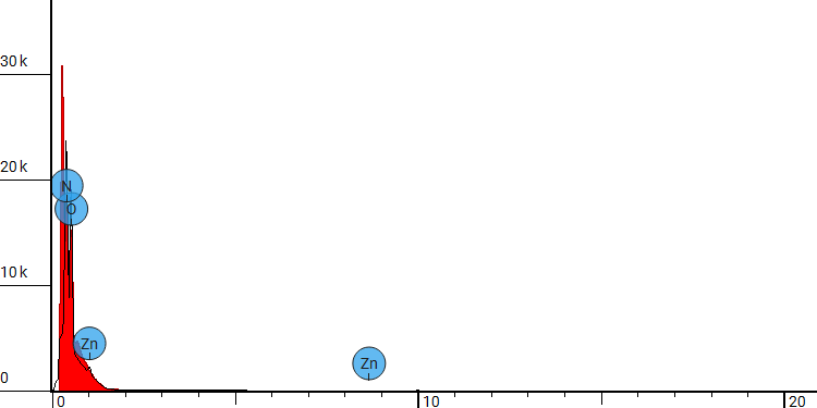 |
| Atomic Number | Symbol | Element | Atomic Concentration (%) | Weight Concentration (%) | Energy Level |
|---|---|---|---|---|---|
| 7 | N | Nitrogen | 0.409436 | 0.366633 | 5300 |
| 8 | O | Oxygen | 0.58124 | 0.594406 | 5300 |
| 30 | Zn | Zinc | 0.00932348 | 0.038961 | 5300 |
I’m not really sure why this is, since hasl should just consist of tin and some lead. I think the nitrogen is still evidence of contamination from my fingers or something. Might need to clean with acetone next time.
HASL vs ENIG surface roughness
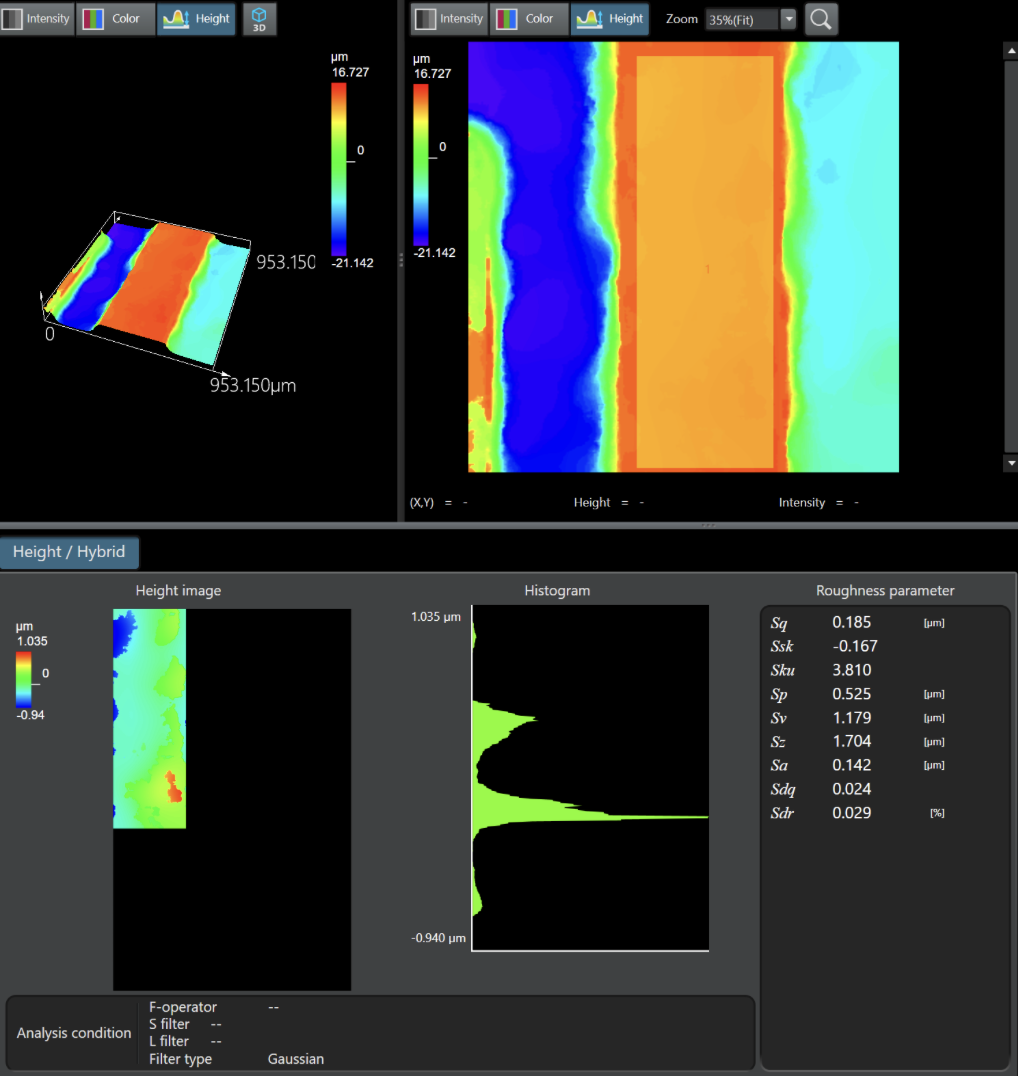
One of the reasons to prefer ENIG to HASL is that it results in a much less rough surface, which avoids loss. As frequency increases, skin depth decreases and a larger proportion of the current density sits in the surface of the trace. For rough surfaces, this means the current essentially travels a longer path length, which is lossy. This is usually described by a factor $K_r$ which modifies the resistance of the line.
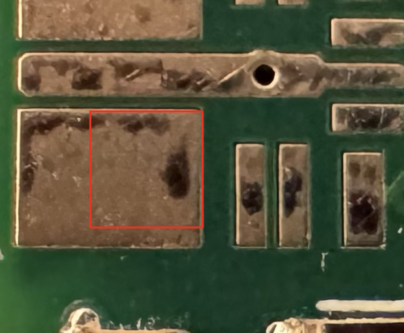
In general, HASL tends to be super uneven because surface level isn’t controlled at all - the board is basically dunked in molten solder, and then cleaned with high pressure air blades. On most HASL boards you can easily see uneven patches of solder - here’s the pad next to the depthmap created by the optical:
 |
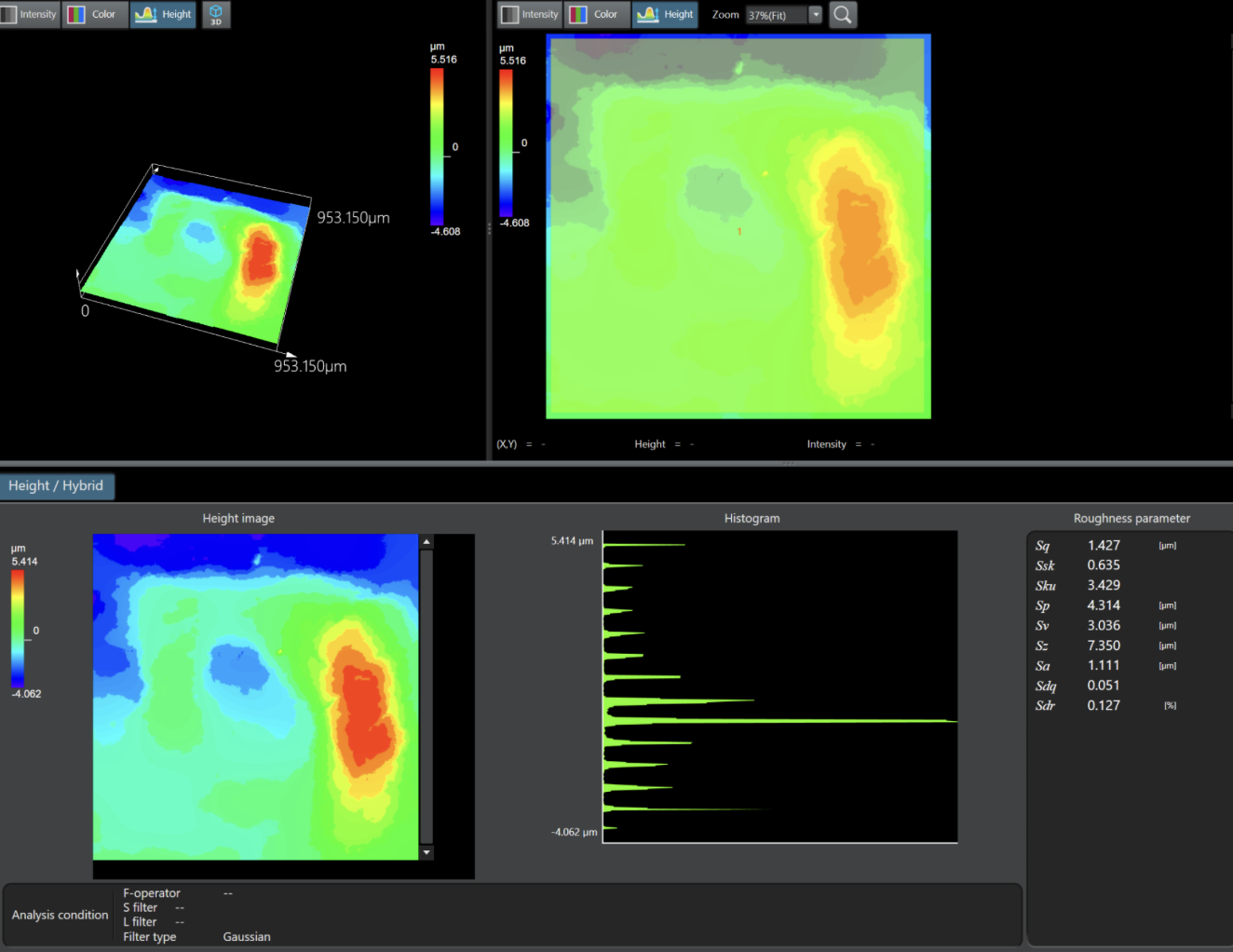 |
$S_q$ RMS surface height. here’s a comparison between a hasl vs enig line section (both from the same TRL board design but with different platings)
| HASL line | ENIG line |
|---|---|
 |
 |
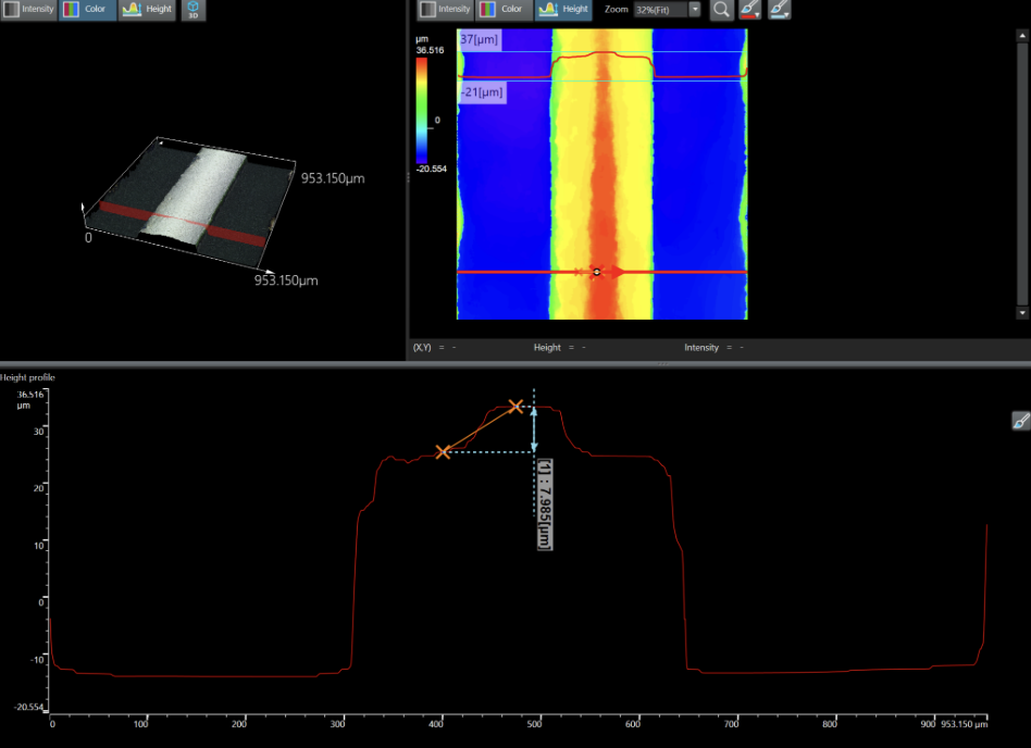
the $S_q$ of the enig is nearly a tenth that of the hasl. Using the hammerstad-jensen model at 5.8ghz in copper, that translates to a 4% increase in resistance against an 80% increase in resistance.
I managed to also find a section of the hasl line where the solder happened to just lie in a patch in the middle. This created a small mountain about 8μm tall:
Main takeaway: do not make rf boards with hasl.
Miscellaneous findings
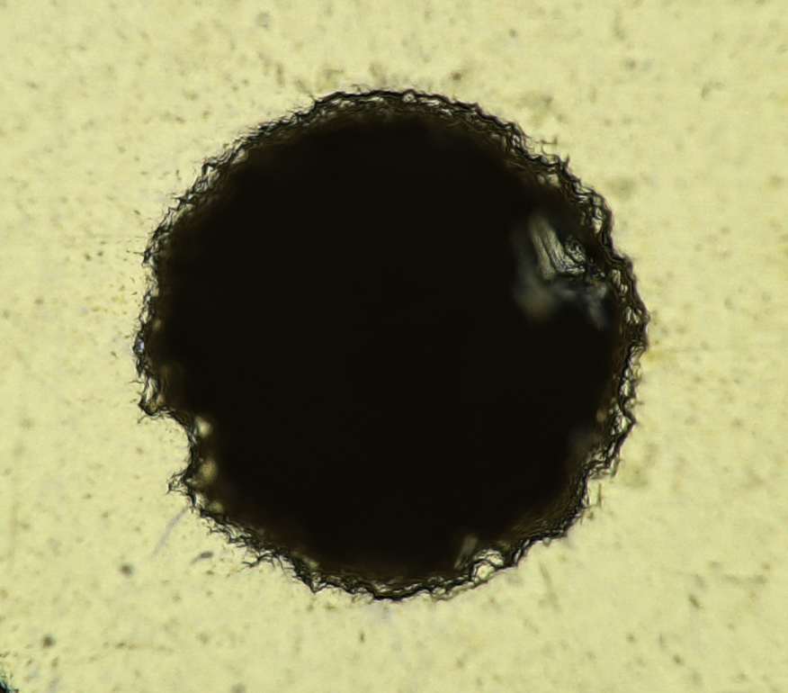
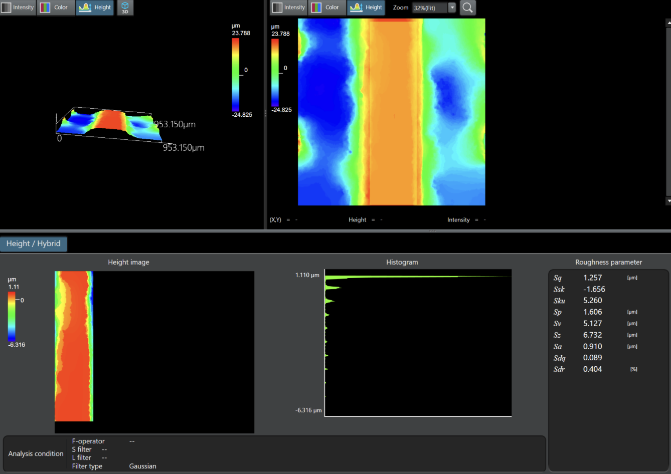
Via annular ring accuracy
On a small section of my sma transition, vias stick out into voided soldermask area. This allows you to easily measure annular ring accuracy:
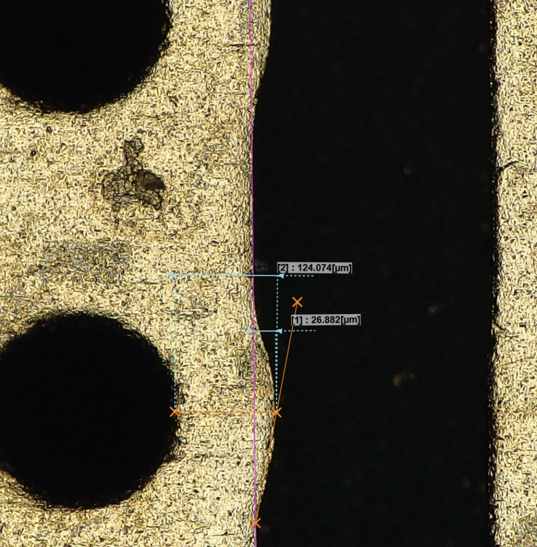
In kicad, I specified an annular ring of 127μm, so safe to say this is accurate. I’m actually surprised they made it exactly as designed since at higher end fabhouses you usually need to adhere to a standardized via + layer stackup for via reliability. I had assumed that jlc did something similar (just had a bunch of via options) but I guess not… jlc doesn’t have a reason to care about long term reliability as much.
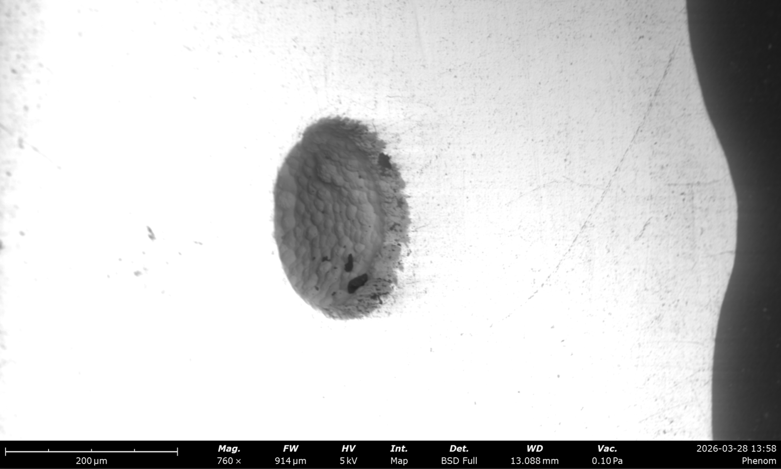
ENIG via nucleation
While doing the above, I noticed that the inside of the enig vias were really bumpy. This is because drilling the via hole creates an extremely rough surface, thereby spawning a bunch of nucleation sites for the nickel to plate to.
Trace undercut
You might notice that to get the picture of the nucleation that the board is actually tilted. That’s because I was trying to get a picture of the via undercut, which is an etching defect in which the sidwalls of traces are slightly concave. Here’s a good diagram, source here:
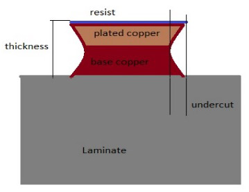
At first I tried to get a depthmap with the optical. This didn’t really work because I had to angle the lens, but the lens was so long that I could only really tilt it around 30 degrees, which didn’t show any undercut. Instead, I used putty to stick the board at an angle on the SEM, which got me some fairly clean pictures:
| HASL undercut | ENIG undercut |
|---|---|
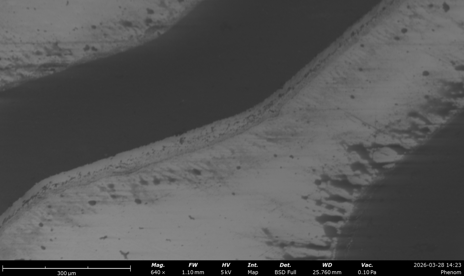 |
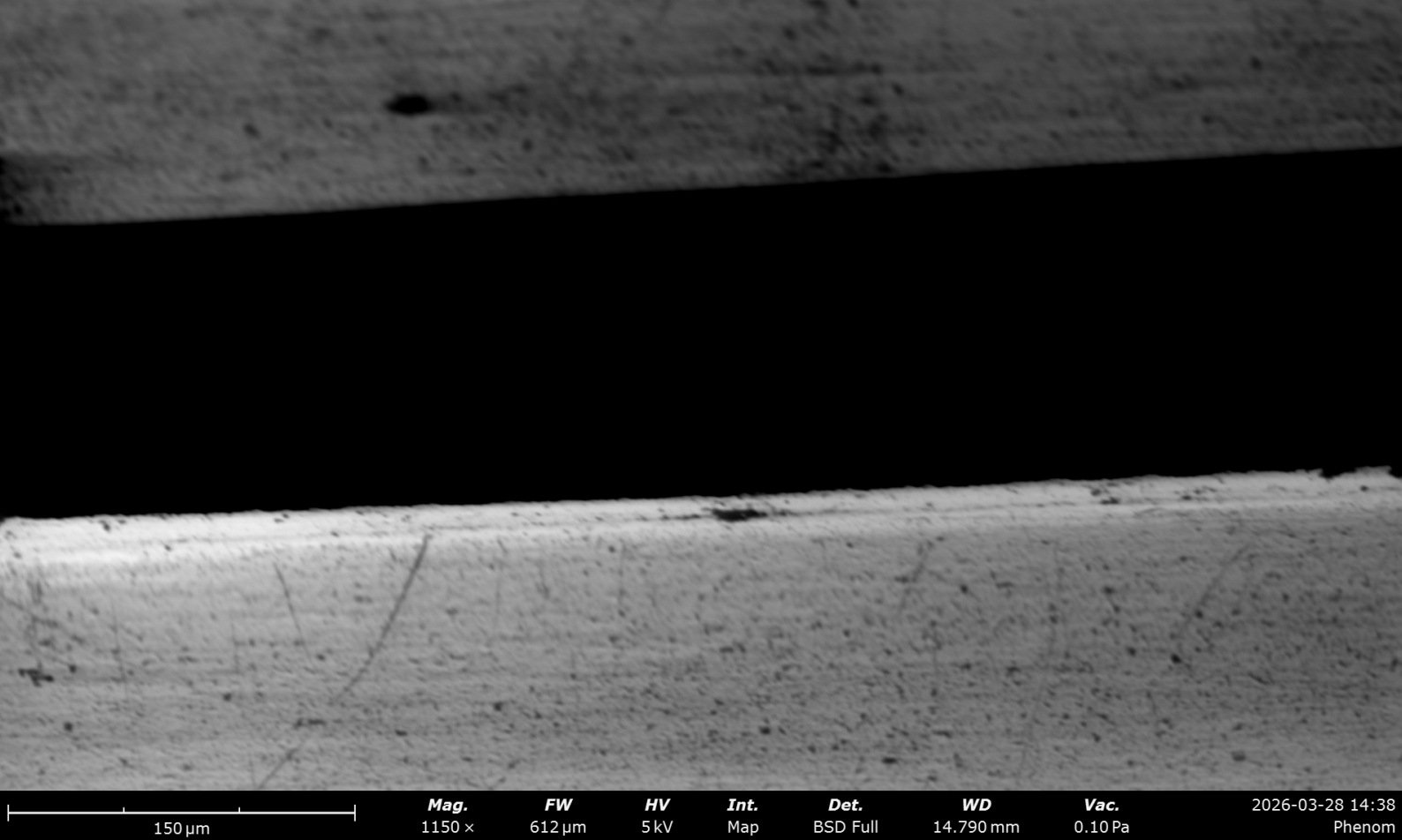 |
Technically the plating shouldn’t make a difference to the undercut, but it seems to me (maybe just because of the setup / quality difference between the two pictures) that the hasl has more undercut. If that’s true, I think it’s probably because the solder is wicking away from the center or so… maybe surface tension… something like that.
Eventually, I want to figure out how to cross section a board / chip and take similar measurements. This is difficult since you need a really accurate grindstone polishing setup, which I don’t think I have access to. Some things it’d be able to do then are get pictures of chip dies and see the full roughness of via walls and internal traces (traces are usually roughened for better bonding to prepreg in an above layer).
Fun experiments!
-
For the record, I took these pictures the day I learned to use the machine. I’ve since discovered that the stage can be rotated and gotten better at the controls to get good top down views… ↩