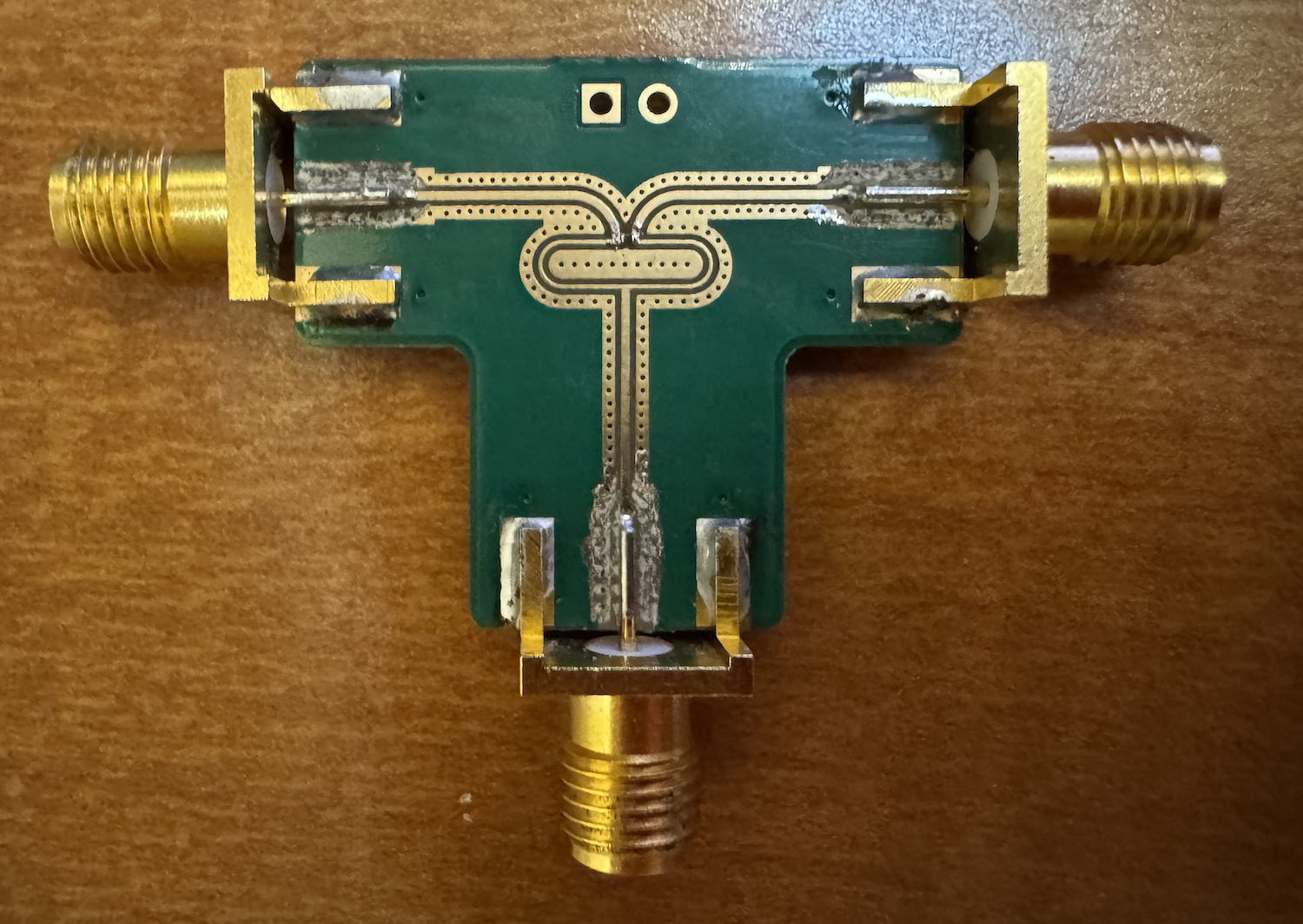
A while ago I made my v1 fmcw radar, which uses a wilkinson power divider to split power from the LO to the tx and the rx mixer 1. As an exercise in validating my hfss simulations (and to also validate the quality of the jlc boards, to the extent that I could) I made a TRL calibration board and a standalone wilkinson tester board:
| TRL boards | Wilkinson |
|---|---|
 |
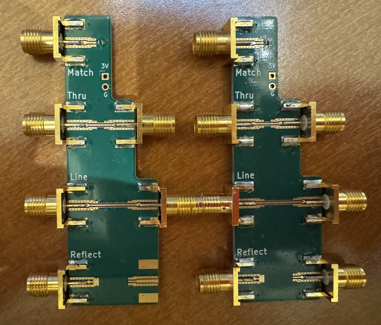 |
Since they were cheap, I had one made with the default jlc stackup and one with the 3313A four layer stackup (which is what the wilkinson + radar are made for) so that I could compare the two.
TRL Calibration
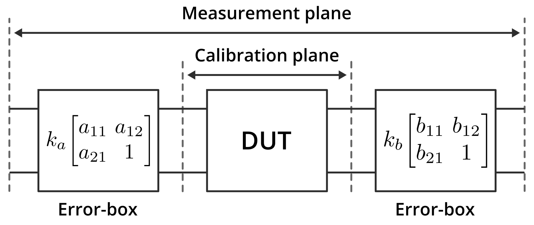
TRL (thru, reflect, line) calibration is used to deembed a DUT from the fixture that it is connected to for measurement. For instance, I was interested in measuring the wilkinson (purely a pcb structure), and used TRL to remove the effect of the VNA, SMA cables, and SMA connector launch up to the structure on the board. TRL (or more generally, line-type calibrations) is popular because it relies on simple standards (the thru, reflect, and line standards) which are easy to make on a pcb. Other calibration methods that rely on standard impedances are difficult to design for wideband operation since the performance of those standards is highly susceptible to parasitics at high frequencies.
I learned the math from Ziad’s article, which explains the process fairly rigorously. TRL compares the thru and line standards (thru is a short transmission line, line is a longer one) to identify what component of the total network is DUT and what is launch / connector / ‘error box.’ This results in an unconstrained system of equations (you only get ratios of $a, b$ to each other), and the reflect is used to resolve the ambiguity (last ‘degree of freedom’) to solve the system.
When I made my cal kit I didn’t know much about the TRL theory (I opted to study it while waiting for the board) so it’s not very good; ideally the difference in electrical length between the thru and line is far from 180 degrees at the center frequency (the difference is not $\lambda / 4 $ since this results in a degenerate case where the matrix is $-I$. The phase margin of my kit is only ~30 degrees; not very good. Of course, any line will be quarter wave at some frequency, so a common workaround to achieve a wideband calibration is to use multiple lines offset such that the difference in electrical length between them is never 180 degrees. This is known as nist multiline trl.
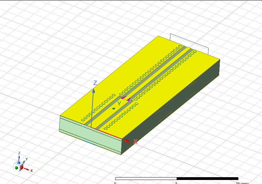
Since I was interested in characterizing my sma transitions, I ended up doing a SLOT calibration on the vna to establish the calibration plane at the end of sma connectors. That way the TRL error boxes would include only the sma edge connector + launch. It also takes care of switch terms. The lines themselves are GCPW with via fencing.
| Default stackup | JLC3313A |
|---|---|
 |
 |
 |
 |
 |
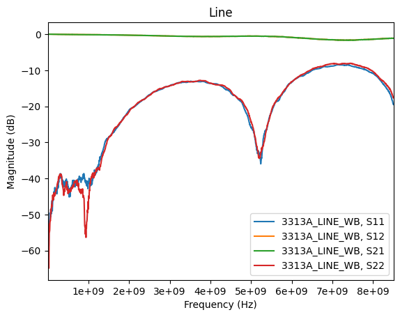 |
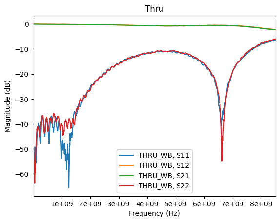
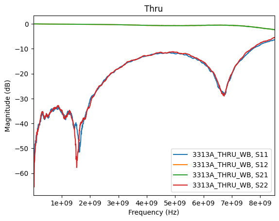
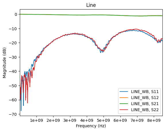
Immediately you can see that there’s some strong resonance going on in the Thru / Line plots. I had simulated the sma transitions, but made a mistake somewhere in reading the impedance of the sma launch and after resimulating it turned out to be 52 ohms. Though the S11 in the simulation was fairly low (<-25db), the resonance didn’t show up because the structure wasn’t periodic (launch-line, not launch-line-launch, which would give resonance between the two mismatched launches). In the plots above, you can see that the return loss starts low and then starts arcing straight up to close to -10db (really bad for a thru).
Substrate analysis
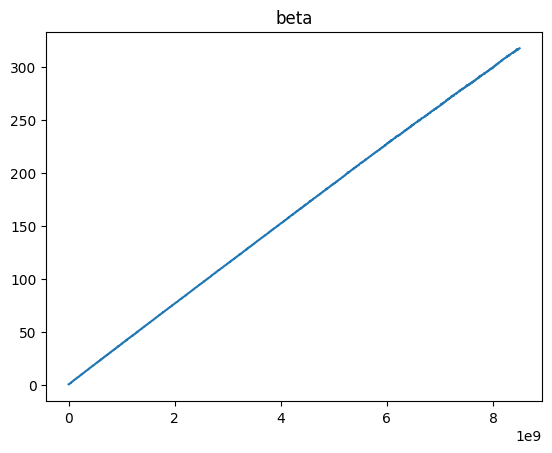
The TRL calibration returns a lot of information about the line. For example, a very clean propagation constant plot. This correlated well with hfss:
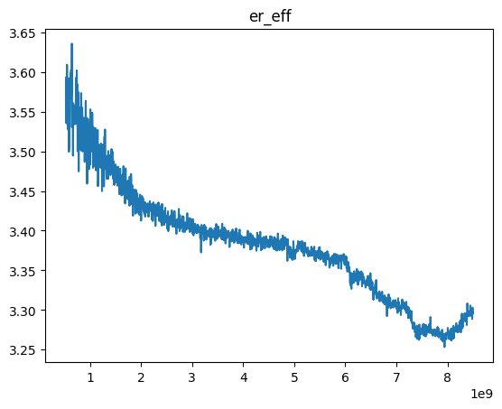
Additionally, it can compute the $\epsilon_{eff}$ of the line. For both stackups:
| Default stackup (dk = 4.4) | JLC3313A (dk = 4.1) |
|---|---|
 |
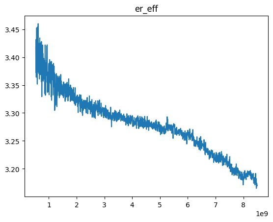 |
The $\epsilon_{eff}$ of the default stackup is only around 0.1 higher than that of the 3313A stackup, but this is expected. For one, the field is split between air and the substrate ($\epsilon_{eff}$ isn’t strictly dependent on dk) and that relation is strongly nonlinear. Just in playing the values in hfss, the difference between dk of 4 and 4.4 only resulted in an $\epsilon_{eff}$ change of 0.8.
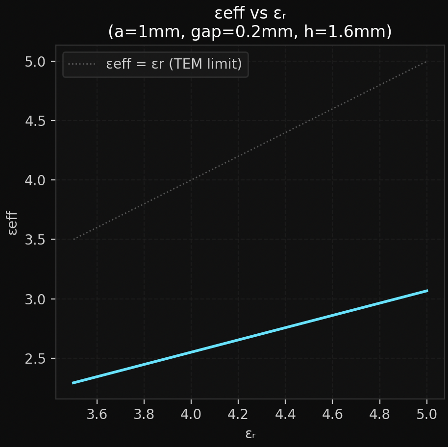
I originally intended to backsolve for the substrate dk based on the effective permittivities I measured, but since GCPW has no closed-form solution, I’d need to do some sort of optimization with a proper field solver and I decided this would be too much work. Instead, I decided that comparing it to GCPW without vias (which has a closed form solution) would be convincing. This is for arbitrary values, but you get the point that the slope is low:
The TRL reported a loss tangent of approximately 0.03 for both stackups, which is in the expected range for FR4. I also emailed jlc about it and they reported 0.02 at 1ghz, and a bit higher is reasonable since $d_f $ increases with frequency.
SMA launch
Since I did a SLOT cal and the TRL calibrates to the center of the thru, the TRL error boxes hold the s parameters of the sma launch:
| measurement | hfss |
|---|---|
 |
 |
You can see that there’s no resonance because the structure isn’t periodic anymore, and though the return losses don’t match up that well, they’re not unreasonably far apart (4db). I can’t really explain that 4db though, aside from the cal maybe not being that accurate due to the resonances.
In an effort to improve the matching, I stuck copper tape under the launch (previously, ground was voided there) in an effort to decrease the impedance ($ Z_{0}\sim\propto \sqrt{ \frac{L}{C} } $) which actually improved the match by 1db ( hard to see on the plot but it’s there):
Z0 extraction (Sketchy)
Starting from the telegrapher’s equations, you can write the wave equation in terms of voltage or current. This will yield the lossy dispersion equation in terms of R, L, G, and C:
\[\gamma = \sqrt{ (R+j\omega L)(G+j\omega C) }\]As an analog to the intrinsic impedance of free space, you can write the impedance of the line in terms of these parameters as well:
\[Z_{0}=\sqrt{ \frac{R+j\omega L}{G+j\omega C} }\]By terminating a line with a resistor you can easily measure the reflection coefficient and thus the Z0 of the line at low frequency (when the resistor reactance can be ignored). At high frequency, $\gamma$ consists of a small real and large imaginary component and $ Z_{0} \approx \sqrt{ \frac{L}{C} } $ so:
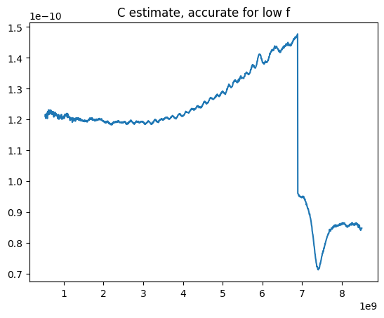
\[\gamma \approx j \omega \sqrt{L_0 C_0} = j \omega C_0 Z_0\]If you pick a frequency that balances such that the reactance of the resistor is still small (so the low frequency Z0 approximation is accurate) but high enough to make the assumptions above, you can solve for $ C_0 $ of the line, which you can assume to be roughly constant over a wide frequency range. From there you can sompute a somewhat accurate Z0 from accurate (measured by TRL) $ \gamma $ and slightly suspicious $ C_0 $ over a wider bandwidth. The following steps in order:
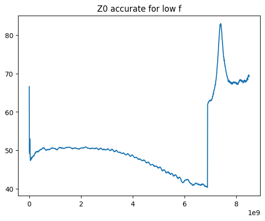
Which reports an impedance very slightly under 50Ohms.
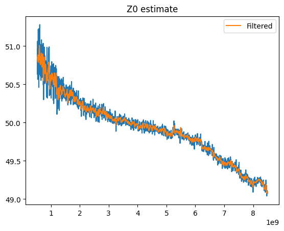
Here is the same procedure run on the board with the default stackup (remember, the only difference is the dk and the geometry is the same)
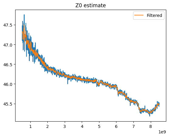
As expected, the impedance is quite a bit lower 2. I think the effect of dk difference is amplified by the inverse term: $ Z_{0}\propto \sqrt{ \frac{1}{\epsilon} } $. Quick hand calc shows that the difference between dk = 3.3, dk=3.2 should yield around a 2% difference in z0 (underestimate because line capacitance is a function only of the dk of the substrate, not the $ \epsilon_{eff} $, which will change more slowly). The difference between the two plots here at 5.8Ghz is around 8%, so this seems… consistent.
Obviously this method will be subject to error, but it at least suggests that the line isn’t widely off. The shape of the curve is also consistent with a line with low loss (rapid dropoff at low frequency) which is what you’d expect for a modern pcb I think.
Z0 extraction (TDR)
Another way to compute the impedance in a network is to use time-domain reflectometry. Traditionally this is done by sending a pulse of voltage, measuring the reflections really quickly and using that to back out the impedances on the line (in a way, similar to getting the impulse response of a system). Turns out that you can also do TDR by taking the inverse fourier transform of the s parameters (measured in the frequency domain). Time resolution is set by the bandwidth of the frequency measurement (higher frequency means finer ‘pulse’ resolution) and the time sweep is set by the number of points.
I ran TDR on the line and thru standards with 1601 points over 8ghz, giving a temporal resolution of 12.5nS. This time resolution isn’t really good enough:
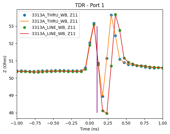
The purple line approximately indicates the end of the line standard (about 1.5cm past the launch) which is when the plot should show 50 ohms. The tdr does actually report this, but accuracy is questionable due to the low resolution. The bigger problem with this output is that the dips right after suggest that the computed impedance is clouded by the impedance of the connector, and you can only really fix that with a different one. Another thing that points to this is that both the Thru and Line match up almost perfectly, which wouldn’t make sense if the tdr actually saw a distinction between the connector and line sections. TDR would probably work here if the line standard was longer.
Standard Z0 extraction
One of the downsides of using TRL is that it establishes the calibration reference impedance as the impedance of the line standard (this is because it assumes that the line has no reflections, thereby enforcing a match3). If this were not the case then it would be possible to compute $Z_0$ directly from S parameters 4:
\[Z_0 =Z_{ref} \sqrt{\frac{(1+S_{11}^2)-S_{21}^2}{(1-S_{11}^2)-S_{21}^2}}\]Instead, TRL will tell you that the impedance of the line is the reference impedance. This is unhelpful since it also doesn’t directly extract the reference impedance, and instead whatever you’re using to compute the TRL will probably default to assigning it the same reference impedance of the S parameters (probably 50 ohms).
For fun, you can easily show that for TRL, $ Z_{ref} = Z_0 $. I applied the cal to my line and computed $\frac{Z_0}{Z_{ref}}$:
thru_caled = cal.apply_cal(thru)

s11 = thru_caled.s[:, 0, 0]
s21 = thru_caled.s[:, 1, 0]

x = np.sqrt(((1 + s11) ** 2 - s21 ** 2) / ((1 - s11) ** 2 - s21 ** 2))
print(x)
Yielded:
[1.-3.46586241e-12j 1.-3.68159943e-10j 1.+1.00538156e-09j ...
 1.-6.95237994e-16j 1.-9.88623722e-17j 1.+1.10455343e-16j]
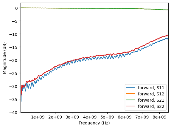
Wilkinson Validation
Once the TRL was finished I started validating the wilkinson. The vna has four ports, but you can only apply a two port TRL to another two port network, so just measured three two ports. scikit-rf has methods to easily combine them, giving the following s parameters:
| Measurement | Sim |
|---|---|
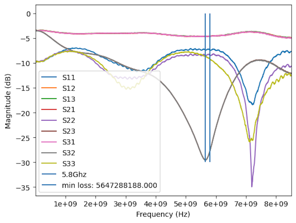 |
 |
The isolation looked great, but the return losses looked bad. Over a few days, I went through a few different theories - that the traces were fabbed wrong, that the sma connector was behaving too reactively (spent a long time trying to model the sma connectors in hfss since most online models are legacy), and some other futile theories. In the end, Will pointed out that the return losses all lined up in the measurements but not in the sim, indicating a resonance. That led to a clear conclusion: the sma ports were all mismatched. I ended up finding a silly mistake - the second layer zone wasn’t filled, completely messing up the GCPW. I ended up resimulating the 50ohm and the 70.7 ohm lines, as well as the sma transitions, and they’d changed to 75, 94, and 54 ohms, respectively (the sma transition had l2 ground voided, so not much actually changed).
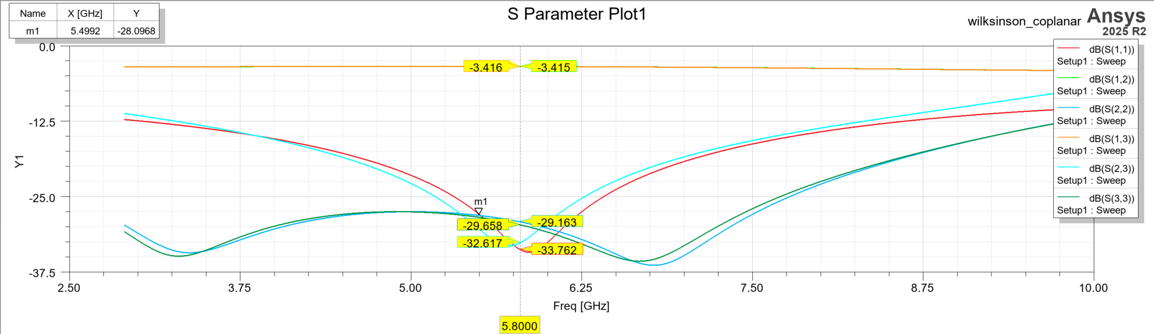
Resimulating the wilkinson gave the following s parameters:
The isolation stayed surprisingly low (since it’s inherently odd mode and the effect of the mistmatches cancelled) but the port 1 return loss got much worse due to the terrible match at the entrance to the T junction. This meant that the resonance was caused by two terrible matches: one at the T junction and one at the sma connector.
I set out trying to at least improve the sma match (now to 75 ohms, not 50). For CPW, $Z_0$ is roughly proportional to the coplanar ground separation from the feedline pad, so over the course of a few hours I ended up cutting a bunch of the ground away from the feedlines on each launch, eventually getting a much better looking response (you can see this in the picture at the top of the page). Once I got to the fencing vias not much changed, and I ended up with this:
I’m not sure why the return loss went so low, but frequency at which the dip occurs was consistent with the one in hfss. More importantly, the reflections at ~7Ghz dropped in magnitude significantly, indicating lower Q due to the improved match. Note that the isolation stayed at a pretty consistent ~6Ghz (as designed), demonstrating that the length of the quarter wave sections was at least correct.
Measurement Correlation
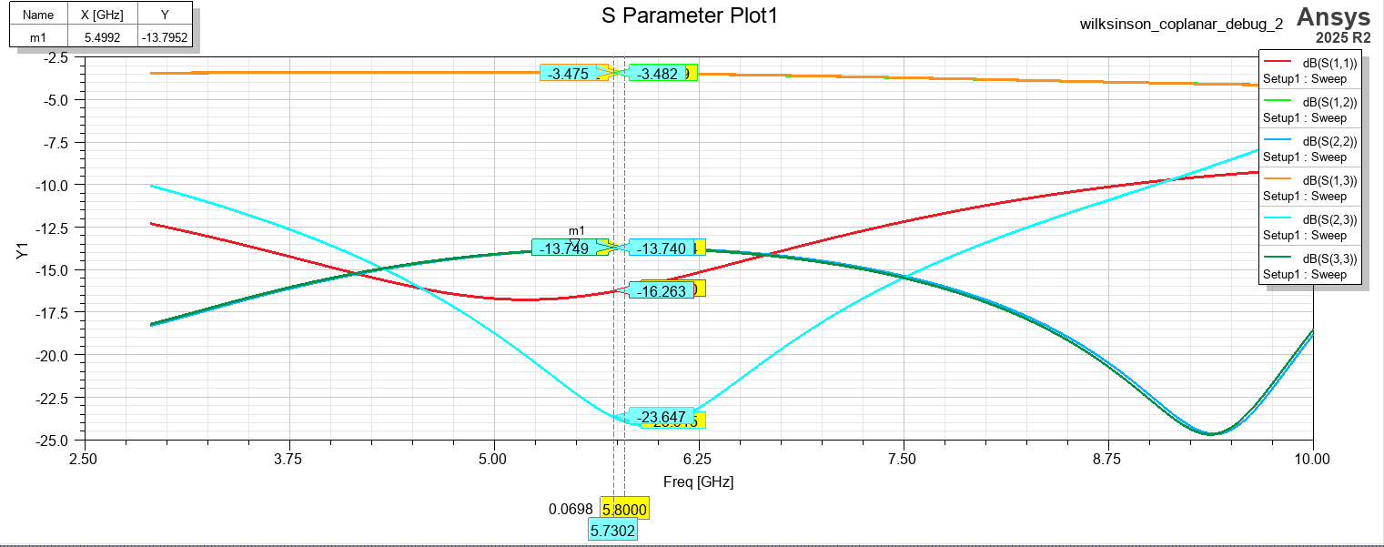
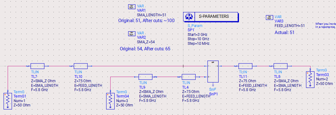
I still wanted to demonstrate that the wilkinson should’ve worked (if L2 Gnd hadn’t been voided) so I correlated the measurements to sim. This consisted of extracting the model of the wilkinson (accurate to what was fabbed) into ads and measuring all the updated line impedances / electrical lengths. In particular, after doing all the cutting on the sma launch, the impedance went to 65 ohms, and the electrical length jumped from 51 degrees to ~103 degrees. You’d expect an increase ($\epsilon_{eff}$ increases with gap spacing since more of the field goes into the dielectric) but an increase of over double was a lot.
Simulating in ADS:
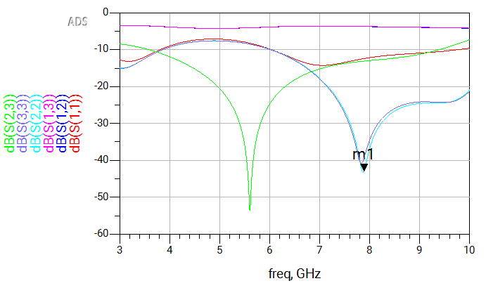
The simulated board after cutting:
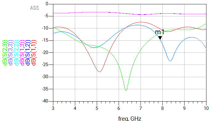
Almost a perfect match. For this type of ad hoc reasoning it’s easy to fall to confirmation bias, but I spent a while checking everything to make sure this was accurate. The simulated ‘before cuts’ matches the response almost perfectly - ‘after cuts’ is slightly less correlated, but close.
The correlation between ads and my measurements made me confident that the wilkinson actually works - at least, that I simulated it right so that hfss and real life agreed.
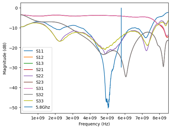
Predicted (real) response
I decided to simulate the wilkinson in ads if an l2 ground existed. This included modeling the sma / line mismatches I discovered with the TRL - that is, this is what I should’ve measured:
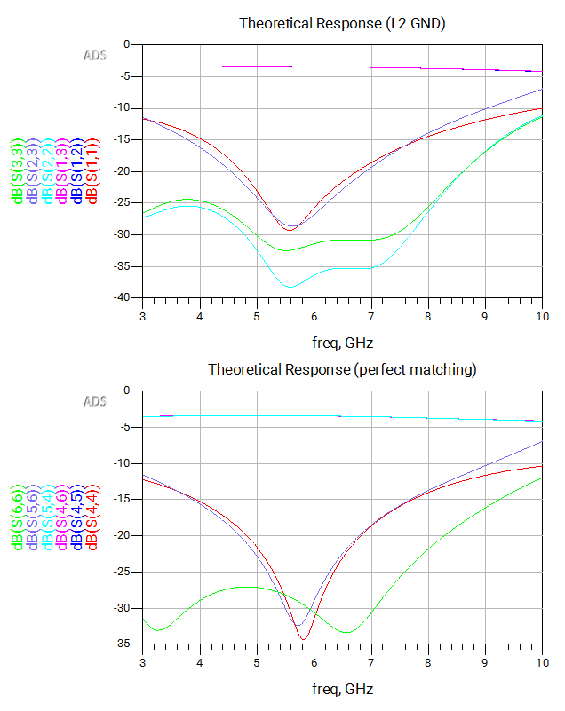
Top plot is that response, bottom is the ideal response (perfect matching). Not bad. I should’ve actually run this sim way before ordering the boards, but didn’t because it takes a while to run on my laptop. I’ll do it next time.
-
Practically it would’ve made more sense to use a coupled line, but a wilkinson is more straightforward mathematically and also seemed cooler. Strictly speaking, it doesn’t really matter since the radar isn’t that high performance anyway. ↩
-
Why lower? In general, $C \propto \epsilon \implies Z_{0}\propto \sqrt{ \frac{1}{\epsilon} }$, so higher dk decreases impedance. ↩
-
Note that obviously there still exists a mismatch between the vna / coax cables and the transmission line, but this is grouped into the error network. In principle, I guess you could try using the method above to compute the characteristic impedance of the error network if you’re reasonably well matched (such that the error box can be approximated by a transmission line - this should be true for most coax launches I think?). But then just use tdr? ↩
-
See Steer’s Microwave And RF Design, Networks book. It’s a good book, but the two methods he describes to compute the characteristic impedance of the line (one is the one I described above, second is using the the smith chart by recognizing a bilinear transform) don’t work with half the calibration methods he goes over (mostly TxL standards, the majority of which inherently set the line standard to the reference impedance of the calculation). ↩